Piezoelectric element and method for manufacturing the same, and ink jet head and ink jet recording apparatus using the piezoelectric element
a piezoelectric element and piezoelectric technology, which is applied in the field of piezoelectric elements and methods for manufacturing the same, and ink jet head and ink jet recording apparatuses using piezoelectric elements, can solve the problems of dielectric breakdown, reduced insulation resistance, and decreased piezoelectric insulation of piezoelectric materials
- Summary
- Abstract
- Description
- Claims
- Application Information
AI Technical Summary
Benefits of technology
Problems solved by technology
Method used
Image
Examples
first embodiment
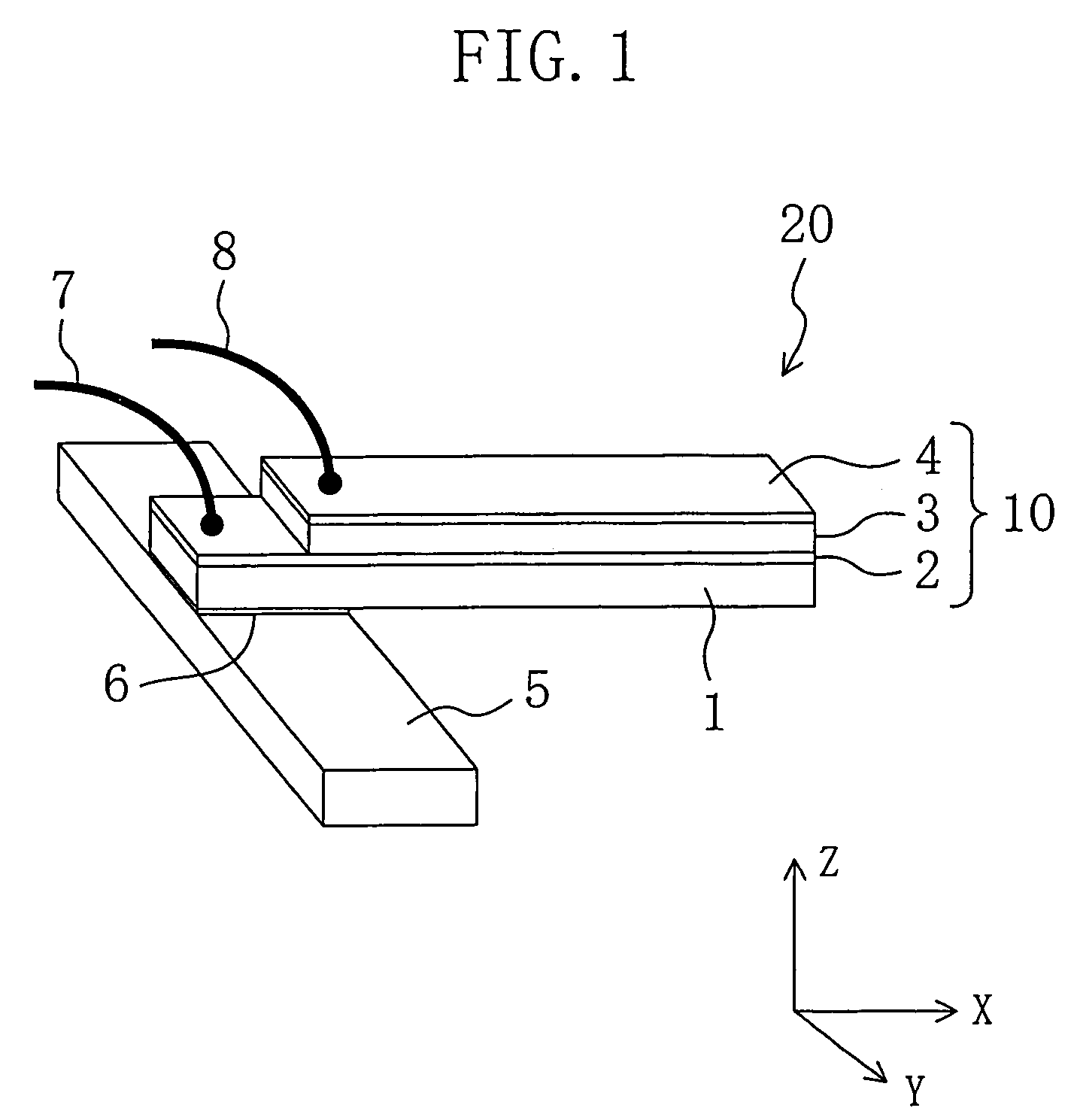
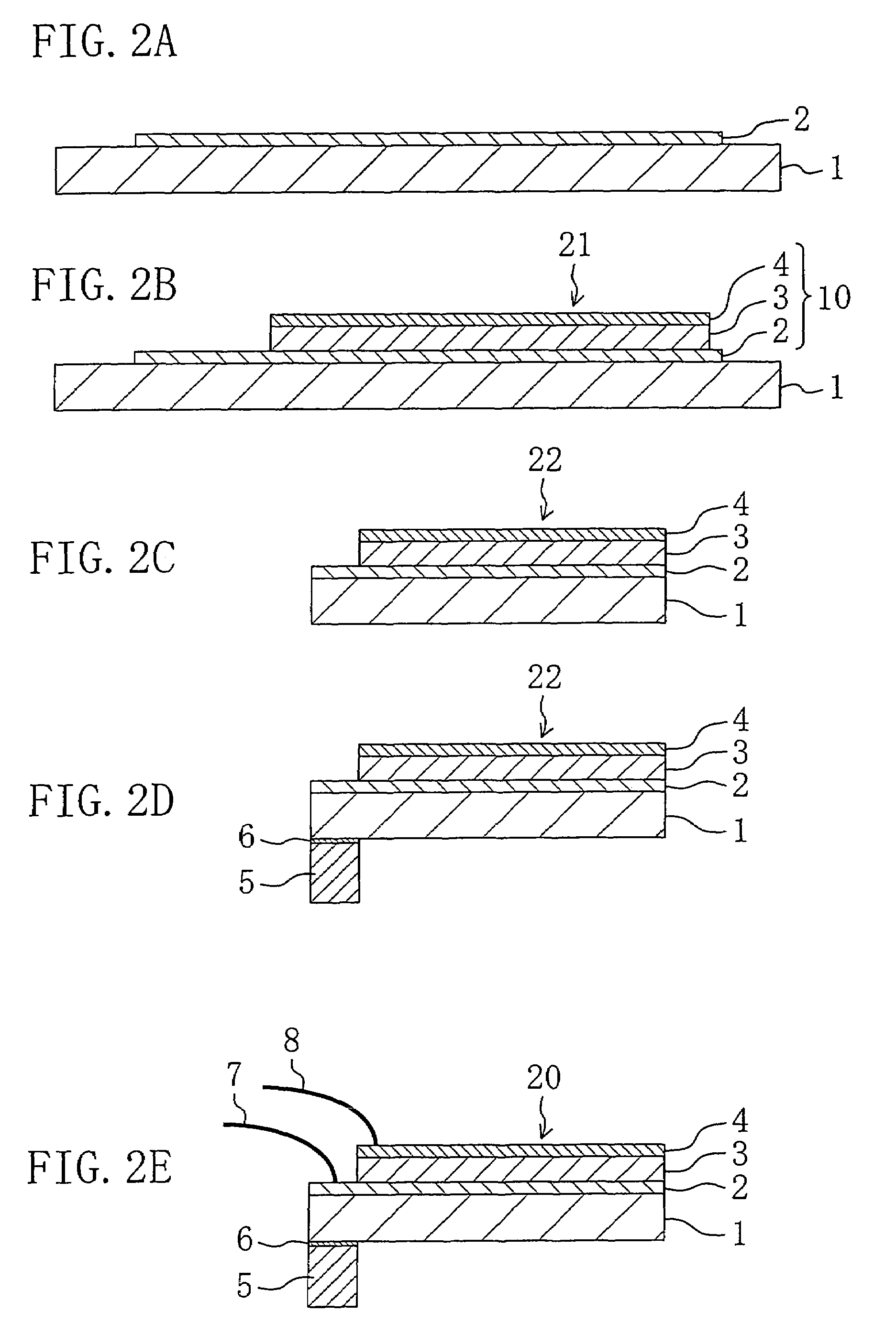
[0056]FIG. 1 is a perspective view illustrating a piezoelectric element according to an embodiment of the present invention. As illustrated in FIG. 1, the piezoelectric element 20 of this embodiment includes a substrate 1 made of flat strip shaped silicon (Si) having a length of 11.0 mm, a width of 3.0 mm, and a thickness of 0.30 mm, and a layered structure 10 provided on the substrate 1. A 3.0-mm end portion of the piezoelectric element 20 is fixed, via an epoxy adhesive 6, to a stainless steel support substrate 5 having a length of 10.0 mm, a width of 3.0 mm, and a thickness of 1.0 mm and extending in the direction perpendicular to the piezoelectric element 20 (i.e., the Y axis direction in the coordinate system of FIG. 1). The piezoelectric element 20 is supported by the stainless steel support substrate 5 to form a cantilever.
[0057]The layered structure 10 includes a first electrode film 2, a piezoelectric thin film 3, and a second electrode film 4 layered in this order, and is ...
example 1
[0077]A substrate 1 was a silicon substrate having the same shape as that employed in the above-described embodiment. As in the above embodiment, a first electrode film 2 was an iridium alloy thin film having a thickness of 0.10 μm and containing 6 mol % of cobalt. Using an RF magnetron sputtering apparatus, the iridium alloy thin film was deposited through a sputtering process by applying a high-frequency power of 200 W to a 6 mol %-cobalt-containing iridium plate serving as the target of the sputtering apparatus for 16 minutes, while keeping the temperature of the silicon substrate at 400° C. in a mixed gas of argon and oxygen (gas volume ratio: Ar:O2=15:1) serving as the sputtering gas at a total gas pressure of 0.25 Pa. In this film deposition process, in the sputtering apparatus, the potential of the silicon substrate was kept electrically floating so as not to be fixed at the ground potential.
[0078]A piezoelectric thin film 3 was a PZT thin film preferentially oriented along t...
example 2
[0090]In this example, the sputtering gas pressure, a sputtering deposition condition employed in formation of a piezoelectric thin film 3 (PZT thin film), was changed to 0.12 Pa, and in the other respects, a piezoelectric element 20 was prepared in the same manner as in Example 1.
[0091]As a result of an analysis by an X-ray diffraction method, it was found that the PZT thin film of the piezoelectric element 20 obtained in this manner was a film having a perovskite crystalline structure and preferentially oriented along the (001) plane (the (001) crystalline orientation degree was 96%). Moreover, results of a composition analysis with an X-ray microanalyzer showed that the composition of the PZT thin film was expressed by Pb(1-x)(Zr(1-s)Tis)O3 where x=0.03 (i.e., Pb0.97(Zr0.53Ti0.47)O3). Furthermore, as a result of observation by a scanning electron microscope, it was found that the thickness of the PZT thin film was 3.5 μm.
[0092]Then, a triangular voltage with a maximum voltage of ...
PUM
| Property | Measurement | Unit |
|---|---|---|
| thickness | aaaaa | aaaaa |
| thickness | aaaaa | aaaaa |
| thickness | aaaaa | aaaaa |
Abstract
Description
Claims
Application Information


