Optical element, optical circuit provided with the optical element, and method for producing the optical element

a technology of optical elements and optical circuits, applied in the direction of optical elements, instruments, optical waveguide light guides, etc., can solve the problems of poor configuration freedom, complicated and sophisticated processing techniques, and unsuitable cwdm awg, so as to reduce coupling loss with optical fibers, reduce polarization dependency, and achieve easy production. high performance

Inactive Publication Date: 2008-03-25
NAT INST OF ADVANCED IND SCI & TECH +1
View PDF7 Cites 22 Cited by
  • Summary
  • Abstract
  • Description
  • Claims
  • Application Information

AI Technical Summary

Benefits of technology

[0023]It is another object of the present invention to provide an optical circuit that has a high wavelength resolution and less dependence on polarization and can be miniaturized, using the optical element.
[0049]Furthermore, a method for producing an optical element of the present invention includes covering at least one surface of a structure having at least one convex portion and at least one concave portion formed so as to be adjacent to either one of the convex portions, wherein the at least one surface of the structure is covered with a covering layer formed by a deposition process. According to this configuration, a hollow portion in a desired shape can be produced. Therefore, an optical element with high performance can be produced easily.

Problems solved by technology

Therefore, even if the AWG is designed for the CWDM, the effects of cost reduction and miniaturization are small, and hence, the AWG is not suitable for the CWDM.
However, according to most of the above-mentioned production methods, a point defect and a line defect are introduced into a particular position.
Therefore, the degree of freedom in terms of configuration is poor.
In order to produce such a configuration, a complicated and sophisticated processing technique is required.
This results in difficulty in miniaturization of an optical demultiplexer.
Furthermore, when the order of diffracted light is increased, it is required to remove unnecessary light of a high order using another apparatus, so that an efficiency is reduced necessarily.
Therefore, even if it is attempted to form a diffraction grating in a slab waveguide, it is difficult to maintain a space for forming the diffraction grating when forming a cladding layer in an upper portion of the slab waveguide.
Furthermore, in order to attach the periodic structures to each other, for example, assuming that a semiconductor is a substrate material, a high-degree and complicated process is required, in which structures are fused to each other in a furnace of 500° C. with a positional precision at nano-level, and repeating this by the number of layers.
Needless to say, a material to be used also is limited to those which can be fused.
Furthermore, it is not easy to enlarge an area.

Method used


Image

  • Optical element, optical circuit provided with the optical element, and method for producing the optical element
  • Optical element, optical circuit provided with the optical element, and method for producing the optical element
  • Optical element, optical circuit provided with the optical element, and method for producing the optical element

Examples


embodiment 1

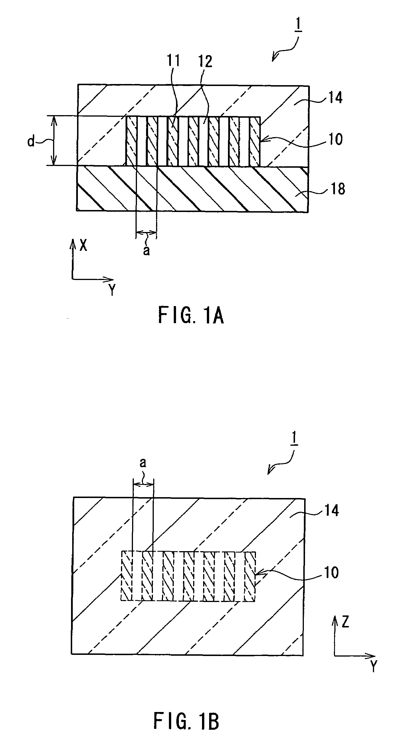
[0094]FIG. 1A is a cross-sectional view showing a configuration of an optical element 1 according to Embodiment 1 of the present invention. FIG. 1B is a plan view of the optical element 1 according to Embodiment 1 of the present invention. A structure 10 includes a substrate 18, ridges 11 that are convex portions formed on the substrate 18, and grooves 12 that are concave portions formed between the ridges 11. The structure 10 is a periodic structure in which the ridges 11 and the grooves 12 are arranged periodically, and a covering layer 14 is formed so as to cover the structure 10. Although the structure 10 is covered with the covering layer 14, the covering layer 14 is not incorporated in the grooves 12, and the grooves 12 are hollow. In FIG. 1B, the structure 10 is not seen due to the covering layer 14; however, the grooves 12 are represented by a broken line for ease of understanding.

[0095]Herein, the periodic structure refers to a periodic arrangement of two kinds of materials...

example 1

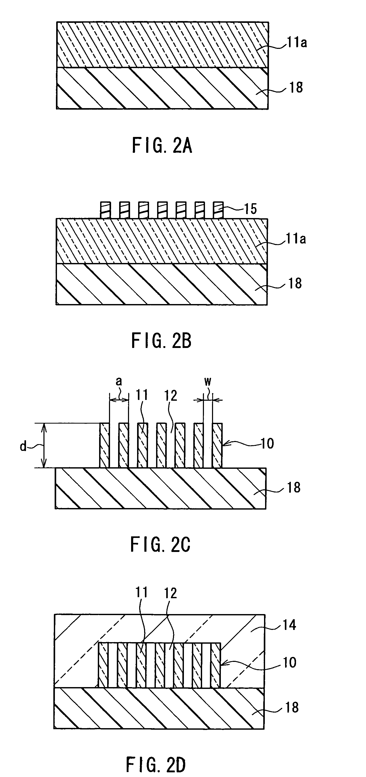
[0113]An optical element 1 with a one-dimensional periodic structure embedded therein was produced by the following procedure, as shown in FIGS. 2A to 2D. Aline-shaped metal mask 15 was formed at an equal interval on a solid material 11a formed on a substrate 18. Thereafter, ridges 11 and grooves 12 were formed of the solid material 11a by dry etching. At this time, the ridges 11 and the grooves 12 were formed alternately so as to have a one-dimensional periodic structure. A period a in the structure 10 thus produced was 3 μm, a groove depth d was 4 μm, and an aspect ratio AR was 3. Silica to be the covering layer 14 was formed on the surface of the structure 10 by plasma CVD. FIG. 3 shows a scanning electron micrograph of a cross-section of the optical element 1 after forming the covering layer 14. As is apparent from FIG. 3, the structure 10 is positioned under the covering layer 14 made of silica. Furthermore, it is confirmed that the covering layer 14 is not incorporated in the ...

example 2

[0119]An optical element 1 of Example 2 according to Embodiment 1 will be described. The optical element 1 of Example 2 is, for example, a high-functional diffraction grating. In the optical element 1 of Example 2, as shown in FIG. 2B, a mask pattern was formed on a solid material 11a, using a metal mask 15 by electron beam drawing and lift-off of Ni. Thereafter, ridges 11 and grooves 12 were formed of the solid material 11a by dry etching of Inductively Coupled Plasma-RIE (ICP-RIE).

[0120]For film formation, RF sputtering was performed, using silica as a target for a covering layer 14. FIG. 4 shows a scanning electron micrograph of a cross-section of the optical element 1 produced in Example 2. A structure 10 is a diffraction grating that is a periodic structure. It is understood from FIG. 4 that the groove width hardly is reduced by film formation, and the covering layer 14 can be suppressed from being incorporated into the grooves 12. The diffraction grating that is the structure ...


PUM


Abstract

An optical element of the present invention includes a structure having at least one convex portion and at least one concave portion formed so as to be adjacent to either one of the convex portions. At least one surface of the structure is covered, and the optical element has a hollow portion. At least one surface of the structure is covered with a covering layer formed by a deposition process.

Description

BACKGROUND OF THE INVENTION[0001]1. Field of the Invention[0002]The present invention relates to an optical element, an optical circuit provided with the optical element, and a method for producing the optical element.[0003]2. Description of the Related Art[0004]Due to the rapid spread of the Internet, there is a strong demand for an increase in the information transmission capacity of an optical fiber communication network. Under such a circumstance, wavelength division multiplexing (WDM) has been developed rapidly. The WDM is a communication technique of multiplexing independent information to transmit it, using light having a plurality of different wavelengths. According to this technique, in order to demultiplex a signal, an optical demultiplexer having a satisfactory wavelength selectivity is required.[0005]In recent years, optical communication by the WDM is applied not only to long distance networks but also to short distance, metropolitan and access networks. In this case, C...

Claims


Application Information

Patent Timeline
Patent Type & Authority Patents(United States)
IPC IPC(8): G02B6/10G02B5/18G02B6/122G02B6/124G02B6/34G02B17/00G02B21/00G02B23/00G02B27/44G02B27/46
CPCB82Y20/00G02B6/1225G02B6/124G02B6/29307G02B6/29311G02B6/2938
Inventor NISHII, JUNJINAKAZAWA, TATSUHIROKITTAKA, SHIGEOTSUNETOMO, KEIJI
Owner NAT INST OF ADVANCED IND SCI & TECH
Why Eureka
Try Eureka