
Method of growing a semiconductor layer

a semiconductor material and epitaxy technology, applied in the direction of polycrystalline material growth, crystal growth process, vacuum evaporation coating, etc., can solve the problem of difficult growth of high-quality gan layers by mbe, difficult to obtain such carrier concentrations, and inability to achieve p-type doping of the material by incorporating magnesium atoms into the semiconductor material, etc. problem, to achieve the effect of increasing the concentration of activated magnesium atoms

Inactive Publication Date: 2008-04-15
SHARP KK
View PDF7 Cites 3 Cited by
  • Summary
  • Abstract
  • Description
  • Claims
  • Application Information

AI Technical Summary

Benefits of technology

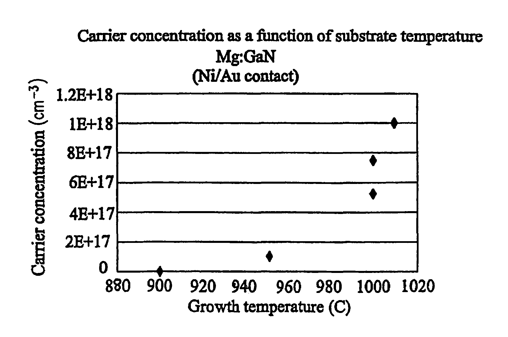
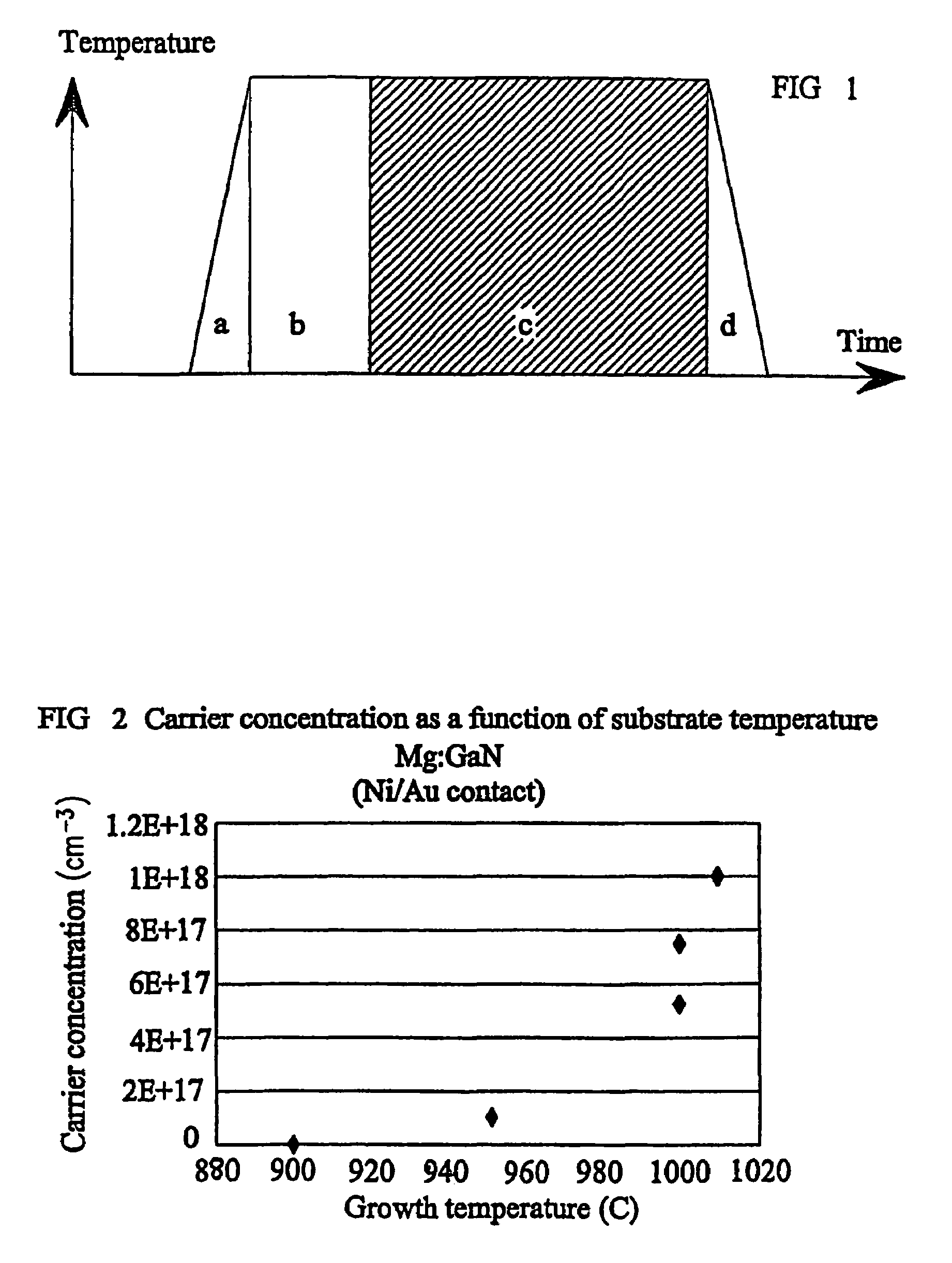
[0014]This method enables the high temperature growth of the nitride semiconductor material, while at the same time providing increased concentration of activated magnesium atoms in the material. As a result, it is possible to grow a p-type doped material that has a free carrier concentration that is sufficiently high for device applications and does not require activation.

Problems solved by technology

Many devices require a free carrier concentration in the p-type doped GaN of at least 1018 cm−3, however, and there have been difficulties in obtaining such carrier concentrations in magnesium-doped GaN.
Thus, incorporating magnesium atoms into a semiconductor material may not achieve p-type doping of the material, and a magnesium-doped semiconductor material may even be n-type.
At present, growing high quality GaN layers by MBE is more difficult than growing such layers by MOCVD.
The principal difficulty is in supplying sufficient nitrogen during the growth process.
Magnesium-doped GaN grown using this method is found to have an acceptable electrical conductivity without the need for an annealing step, but this particular growth method is not relevant to MBE growth.
However, the growth conditions used are such that, although magnesium is incorporated into the gallium nitride, p-type doping is not shown to be achieved.

Method used


Image

  • Method of growing a semiconductor layer
  • Method of growing a semiconductor layer
  • Method of growing a semiconductor layer

Examples


Embodiment Construction

[0032]One example of a growth method according to the present invention, illustrating the growth of a p-type doped nitride layer having magnesium as a p-type dopant, will now be described. In this embodiment the nitride layer is a p-type GaN layer, but the invention is not limited to the growth of p-type GaN.

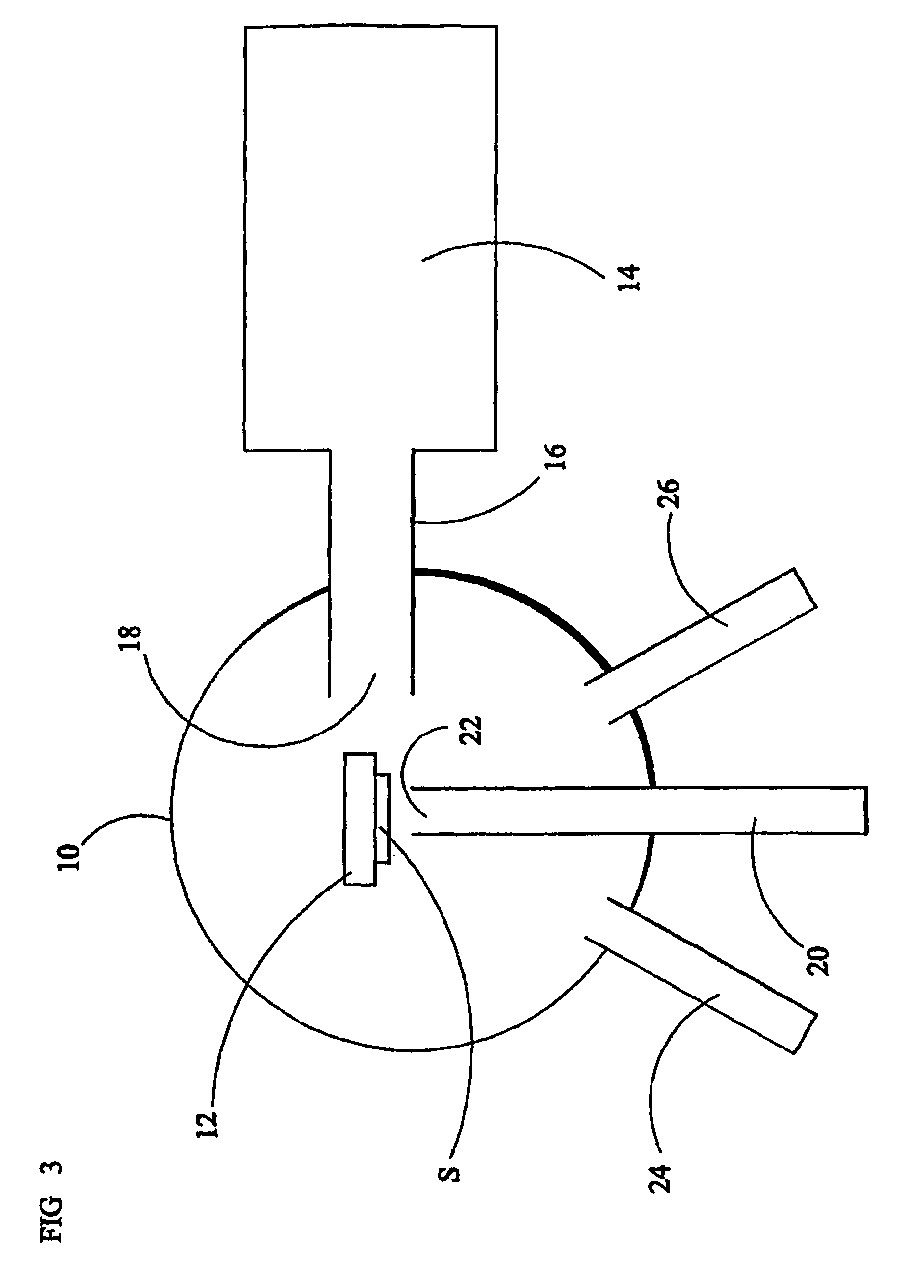
[0033]A suitable substrate is prepared in any conventional manner, and is introduced into the growth chamber of an MBE apparatus. The substrate is preferably a GaN substrate. A GaN substrate for use in the epitaxial growth of GaN can have two possible forms—it maybe a “free-standing” substrate, or a “template” substrate. A free-standing GaN substrate consists solely of GaN, and is formed by, for example, a GaN crystal. A template GaN substrate consists of a thick epitaxial layer of GaN grown on a base substrate of, for example, sapphire or silicon carbide. The thick epitaxial layer is grown on the base substrate by any suitable technique such as metal-organic vapour phase epitax...


PUM

PropertyMeasurementUnit
Temperatureaaaaaaaaaa

Abstract

A method of growing a p-type nitride semiconductor material having magnesium as a p-type dopant by molecular beam epitaxy (MBE), comprises supplying ammonia gas, gallium and magnesium to an MBE growth chamber containing a substrate so as to grow a p-type nitride semiconductor material over the substrate. Magnesium is supplied to the growth chamber at a beam equivalent pressure of at least 1 10-9 mbar, and preferably in the range from 1 10-9 mbar to 1 10-7 mbar during the growth process. This provides p-type GaN that has a high concentration of free charge carriers and eliminates the need to activate the magnesium dopant atoms by annealing or irradiating the material.

Description

TECHNICAL FIELD[0001]This invention relates to a molecular beam epitaxy (MBE) method for the epitaxial growth of Group III nitride semiconductor materials such as, for example, GaN. It particularly relates to the growth of a p-type doped nitride semiconductor material in which magnesium is the p-type dopant.BACKGROUND ART[0002]Many electronic devices and optoelectronic devices are based on the GaN material family. These devices require at least one interface between an n-type doped material and a p-type doped material, in order to form a p:n junction and / or allow injection of electrical carriers into the device. GaN is naturally an n-type doped semiconductor material, and p-type doped GaN is obtained by introducing a suitable dopant species during the GaN growth process. Magnesium is often used as a p-type dopant for GaN. Many devices require a free carrier concentration in the p-type doped GaN of at least 1018 cm−3, however, and there have been difficulties in obtaining such carrie...

Claims


Application Information

Patent Timeline
IPC IPC(8): H01L21/00C23C14/06C30B23/02C30B29/38H01L21/203H01L33/32
CPCC30B23/02H01L21/02389H01L21/0254H01L21/02579H01L21/02631C30B29/40H01L21/0237H01L21/02458Y10S438/933
Inventor BARNES, JENNIFER MARYBOUSQUET, VALERIEHOOPER, STEWART EDWARDHEFFERNAN, JONATHAN
Owner SHARP KK
Learn More