Fabrication method of high-brightness light emitting diode having reflective layer

a technology of light-emitting diodes and fabrication methods, which is applied in the direction of basic electric elements, electrical apparatus, and semiconductor devices, can solve the problems of reduced reflectivity, limited brightness, and reduced external quantum efficiency of leds, and achieves reduced resistance, improved reflectivity, and maintained reflective surface flatness

Active Publication Date: 2008-06-10
EPISTAR CORP
View PDF13 Cites 22 Cited by
  • Summary
  • Abstract
  • Description
  • Claims
  • Application Information

AI Technical Summary

Benefits of technology

[0014]A significant characteristic of the present invention lies in the deposition of the non-alloy ohmic contact layer and the first metallic layer in resolving the substrate absorption problem. The first metallic layer functions as a reflective mirror and is made of a pure metal or a metal nitride for superior reflectivity. The non-alloy ohmic contact layer is interposed between the light generating structure and the first metallic layer so as to achieve the required low resistance electrical conduction. To prevent the first metallic layer from intermixing with the non-alloy ohmic contact layer and the light generating structure, and to maintain the flatness of the reflective surface of the first metallic layer, the present invention farther comprises a step to interpose an optically transparent and electrically conductive first dielectric layer between the first metallic layer and the non-alloy ohmic contact layer.
[0015]Another significant characteristic of the present invention lies in that the reflective surface of the reflective mirror (i.e., the first metallic layer) does not directly participate in the wafer-bonding process. The first metallic layer is directly coated to the light generating structure in vacuum during the preparation of the first layered structure and it is the bottom surface of the first metallic layer involving in the subsequent wafer-bonding process. Therefore, the exposure to the air, the high annealing temperature and pressure of the wafer-bonding process would not cause contamination to the reflective surface of the first metallic layer and thereby compromise the surface flatness and reflectivity of the first metallic layer. To achieve superior bonding between the second substrate and the first metallic layer, the present invention could further comprise a step of depositing at least an additional metallic layer beneath the first metallic layer, or on top of the second substrate, or both, to function as a bonding agent. Similarly, if the additional metallic layer is formed beneath the first metallic layer, to prevent it from intermixing with the first metallic layer and thereby compromising the reflectivity of the first metallic layer, the present invention could interpose a second dielectric layer between the first metallic layers and the additional metallic layer.

Problems solved by technology

However, the DBRs provide high reflectivity only for normal incident lights and the reflectivity decreases as the lights' incident angle increases.
The improvement to the LED's external quantum efficiency and brightness is therefore limited.
However, the problem with the approach using transparent substrate is that its wafer-bonding process requires to be operated under a high annealing temperature over an extended period of time, which would cause redistribution of doping profile and degrade the LED's performance.
The problem with the approach using mirror is that the mirror's reflective surface is directly involved in the bonding interface during the wafer-bonding process, which would lead to roughness of the reflective surface or reactions and contaminations to the mirror's reflective surface.
However, alloy material AuBe possesses inferior reflectivity and thereby limits the brightness improvement of the LED.
The alloy process, which usually requires a high annealing temperature, would also compromise the surface flatness of the reflective mirror and degrade its reflectivity.
The disclosed structure has rather complicated fabrication process, and therefore a high production cost.
The alloy metal mesh requires a high temperature alloy process, and etching the alloy metal to form mesh is also very difficult to control.
In addition, the thickness of the alloy metal requires special attention.
If the alloy metal is too thin, the ohmic contact between the alloy metal and the light generating structure is inferior; if the alloy metal is too thick, the wafer bonding process couldn't achieve a strong bonding.

Method used


Image

  • Fabrication method of high-brightness light emitting diode having reflective layer
  • Fabrication method of high-brightness light emitting diode having reflective layer
  • Fabrication method of high-brightness light emitting diode having reflective layer

Examples


Embodiment Construction

[0023]The following descriptions are exemplary embodiments only, and are not intended to limit the scope, applicability, or configuration of the invention in any way. Rather, the following description provides a convenient illustration for implementing exemplary embodiments of the invention. Various changes to the described embodiments may be made in the function and arrangement of the elements described without departing from the scope of the invention as set forth in the appended claims.

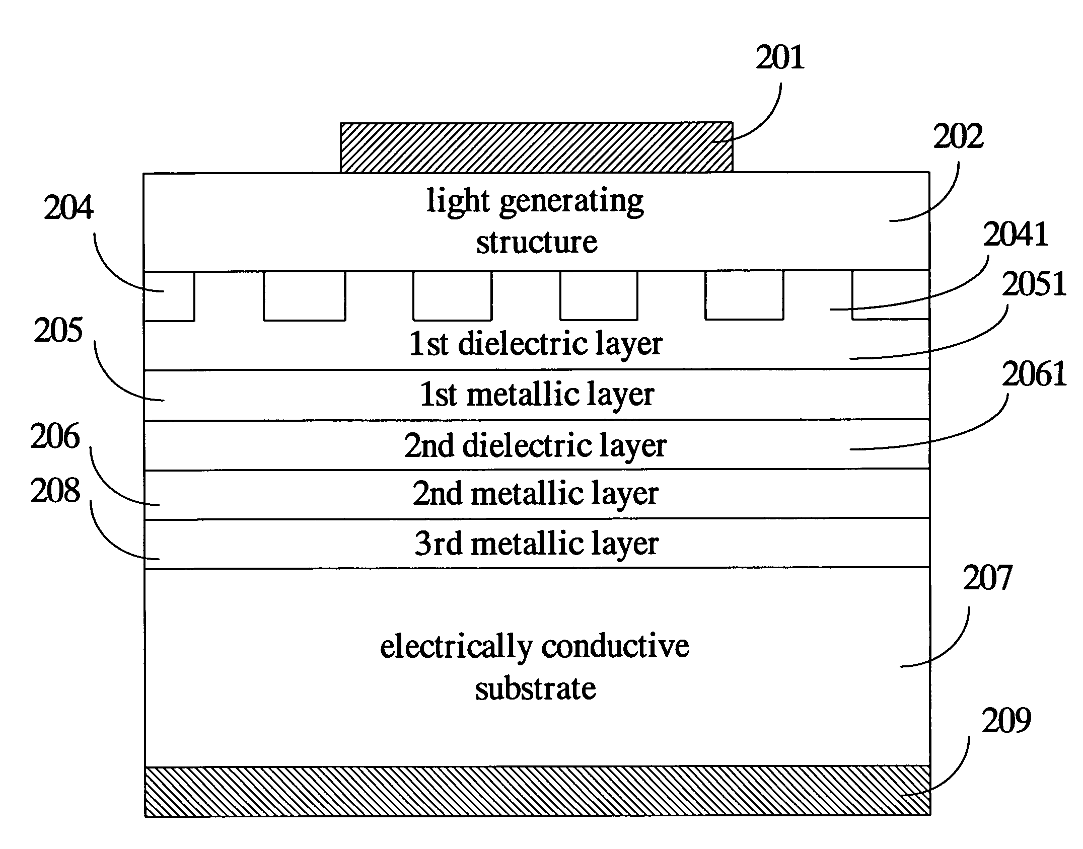
[0024]The present invention generally comprises at least the following steps. First, a first layered structure is provided by sequentially forming a light generating structure, a non-alloy ohmic contact layer, and a first metallic layer from bottom to top on a side of a first substrate. Then, a second layered structure comprising at least a second substrate is provided. Then, the two-layered structures are wafer-bonded together, with the top side of the second layered structure interfacing with the...


PUM


Abstract

A method for fabricating a high brightness LED structure is disclosed herein, which comprises at least the following steps. First, a first layered structure is provided by sequentially forming a light generating structure, a non-alloy ohmic contact layer, and a first metallic layer from bottom to top on a side of a first substrate. Then, a second layered structure comprising at least a second substrate is provided. Then, the two-layered structures are wafer-bonded together, with the top side of the second layered structure interfacing with the top side of said first layered structure. The first metallic layer functions as a reflective mirror, which is made of a pure metal or a metal nitride to achieve superior reflectivity, and whose reflective surface does not participate in the wafer-bonding process directly.

Description

BACKGROUND OF THE INVENTION[0001]1. Field of the Invention[0002]The present invention generally relates to light emitting diodes, and more particularly to a fabrication method for light emitting diodes having a reflective layer to avoid light absorption by the diode's substrate.[0003]2. The Prior Arts[0004]FIG. 1a is a schematic sectional view showing a typical structure of a conventional light emitting diode (LED). As illustrated, the LED 100 contains a semiconductor substrate 103 and a light generating structure 102 on top of the substrate 103, and two ohmic contact electrodes 109 and 101 formed on the other side of the substrate 103 and on top of the light generating structure 102 respectively.[0005]The light generating structure 102 is often made of layers of aluminum-bearing III-V compound semiconductors, such as AlGaAs for infrared and red lights, AlGaInP for yellow-green, yellow, amber, and red lights. The substrate 103 is usually made of gallium arsenide (GaAs) which has a m...

Claims


Application Information

Patent Timeline
Patent Type & Authority Patents(United States)
IPC IPC(8): H01L21/00H01L33/00H01L33/38H01L33/40
CPCH01L33/387H01L33/405H01L33/0079H01L33/0093
Inventor LIU, JIN-HSIANGWANG, HUI-HENGLIN, KUN-CHUAN
Owner EPISTAR CORP
Why Eureka
Try Eureka