Semiconductor device

a technology of semiconductor devices and metal films, applied in the direction of semiconductor devices, semiconductor/solid-state device details, diodes, etc., can solve the problems of difficult patterning of high melting point metal films by dry etching technology, difficult to prevent connection holes, and over-etching (excessive etching) to achieve the effect of reducing power, reducing damage, and easy diffusion

Inactive Publication Date: 2008-09-16
RICOH KK
View PDF16 Cites 7 Cited by
  • Summary
  • Abstract
  • Description
  • Claims
  • Application Information

AI Technical Summary

Benefits of technology

[0108]According to the first aspect of the present invention, the underground insulator film of the metal thin-film-resistor object includes a silicon oxide film that contains phosphor, or phosphor and boron at least as the uppermost layer. By using one of a PSG film and a BPSG film that have lower atomic density than an NSG film as the insulator layer contacting the undersurface of the metal thin-film-resistor object, the metal thin-film-resistor object can be easily diffused in the underground insulator film when trimming; accordingly, lower power is required, reducing damage due to laser irradiation of regions adjacent to the metal thin-film-resistor object.
[0109]Further, according to the first aspect of the present invention, the metal thin-film-resistor object is formed on the underground insulator film and inside of the connection hole formed in the underground insulator film, and is electrically connected to the metal wiring pattern formed on the lower layer side insulator film in the connection hole. Accordingly, the patterning process by wet etching technology after forming the metal thin-film-resistor object is not required, which process is necessary in the conventional technology described with reference to FIGS. 37 through 39. Further, since the surface of the metal thin-film-resistor object contacting the metal wiring pattern is not exposed to the atmosphere, a stable and reliable electrical connection between the metal thin-film-resistor object and the metal wiring pattern can be obtained even if a process of removing an oxide film removal process and a process of forming a barrier film for preventing the metal thin-film-resistor object from etching are not performed. In this manner, the metal thin-film-resistor object that is miniaturized and provides a stable resistance can be realized regardless of the thickness of the metal thin-film-resistor object without increasing the number of processes.
[0110]Further, as for the first aspect of the present invention, if at least the upper end of the connection hole is formed in the shape of a taper, the Ar sputter etching residual substance contains at least the materials of the metal wiring pattern and the underground insulator film, and Ar is formed in the inner wall of the connection hole, the Ar sputter etching residual substance improves the step coverage of the metal thin-film-resistor object inside the connection hole, and the contact resistance between the metal wiring pattern and the metal thin-film-resistor object is stabilized. Further, the taper shape of the connection hole, formed at least at the upper end, prevents an overhang of the metal thin film deposited near the upper end of the connection hole from forming when forming the metal thin film for the metal thin film resistance object such that an influence affecting deposition of the metal thin film inside the connection hole is reduced. In this way, the step coverage of the metal thin-film-resistor object can be raised.
[0111]Further, a conventional metal thin-film-resistor object tends to receive influence from its underground film, e.g., resistance fluctuation, as the time elapses from formation of the underground film and due to structure of the underground film. In this connection, the Ar sputter etching process carried out on the underground insulator film according to the present invention is effective to mitigate the underground film dependability of the sheet resistance of the metal thin-film-resistor object, and to reduce the resistance fluctuation with time. As described above, the taper form of the upper end of the connection hole, and the Ar sputter etching residual substance are formed by performing the Ar sputter etching process after forming the connection hole; and the Ar sputter etching process is carried out on the underground film before forming the metal thin film for the metal thin-film-resistor object.
[0112]Effects obtained by the Ar sputter etching process on the underground film of the metal thin-film resistance object are described below.
[0113]According to the semiconductor device of the second aspect of the present invention, since the underground insulator film of the metal thin-film-resistor has the silicon oxide film that contains phosphor, or phosphor and boron at least as the uppermost layer, damage to regions adjacent to the metal thin-film-resistor object by laser irradiation is reduced as in the first aspect of the present invention.

Problems solved by technology

However, since the metal thin-film-resistor object 101, which is thin, is present directly under the metal film for wiring, over-etching (excessive etching) may take place if the dry etching technology is used.
However, where the metal thin-film-resistor object 101 is thinner than 100 nm (1000 Å), it is difficult to prevent the connection holes 107 from running through the metal thin-film-resistor object 101.
Here, since the high melting point metal film is formed immediately above the metal thin-film-resistor object 101, patterning of the high melting point metal film by dry etching technology is difficult.
That may cause damage to the silicon substrate, and the reliability of the semiconductor device may be degraded, which is a problem.
The electron hole pair generates noise that hinders correct measurement, and precise trimming cannot be obtained, which is a problem.

Method used


Image

  • Semiconductor device
  • Semiconductor device
  • Semiconductor device

Examples


Embodiment Construction

[0044][Problem(s) to be Solved by the Invention]

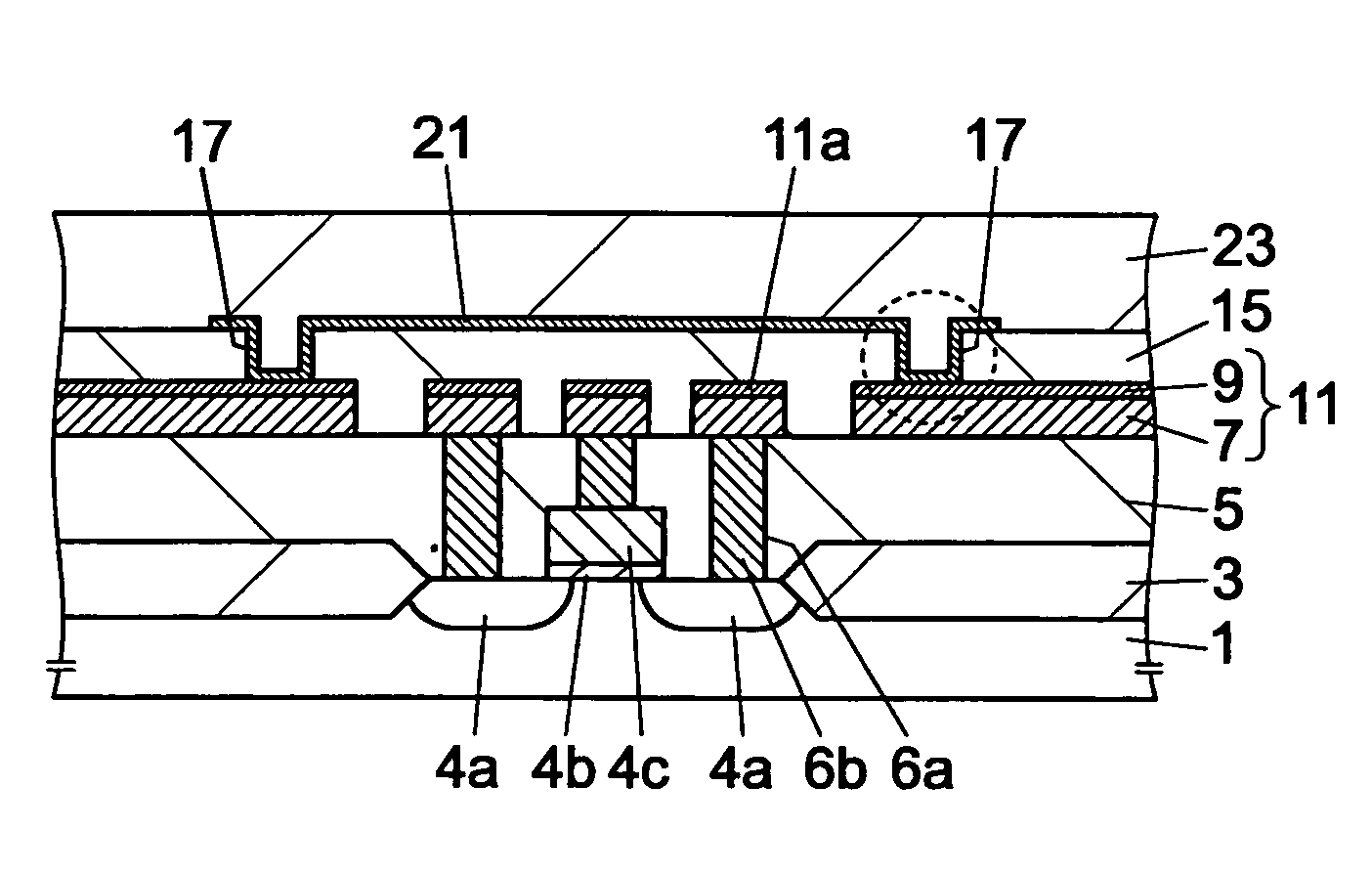
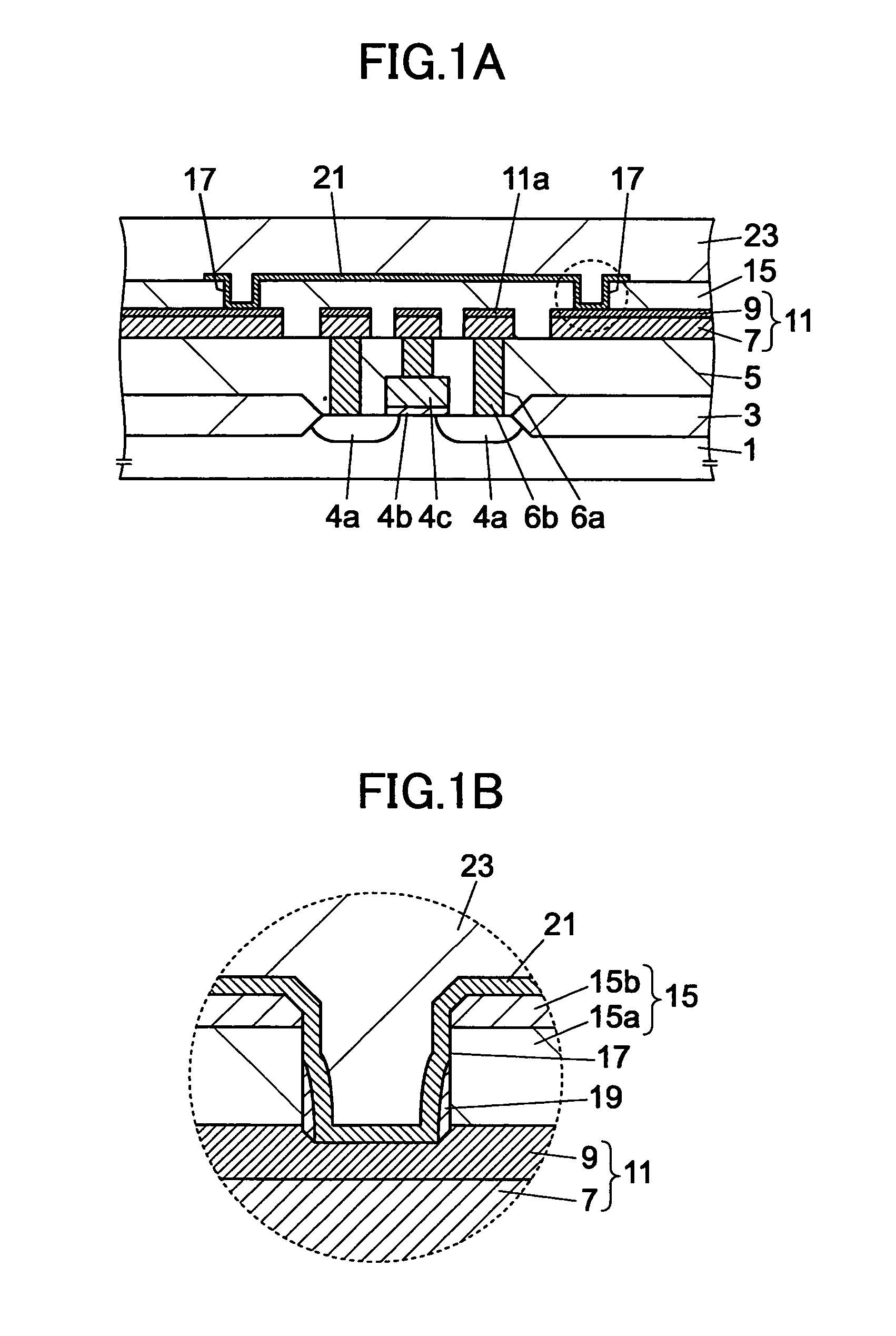
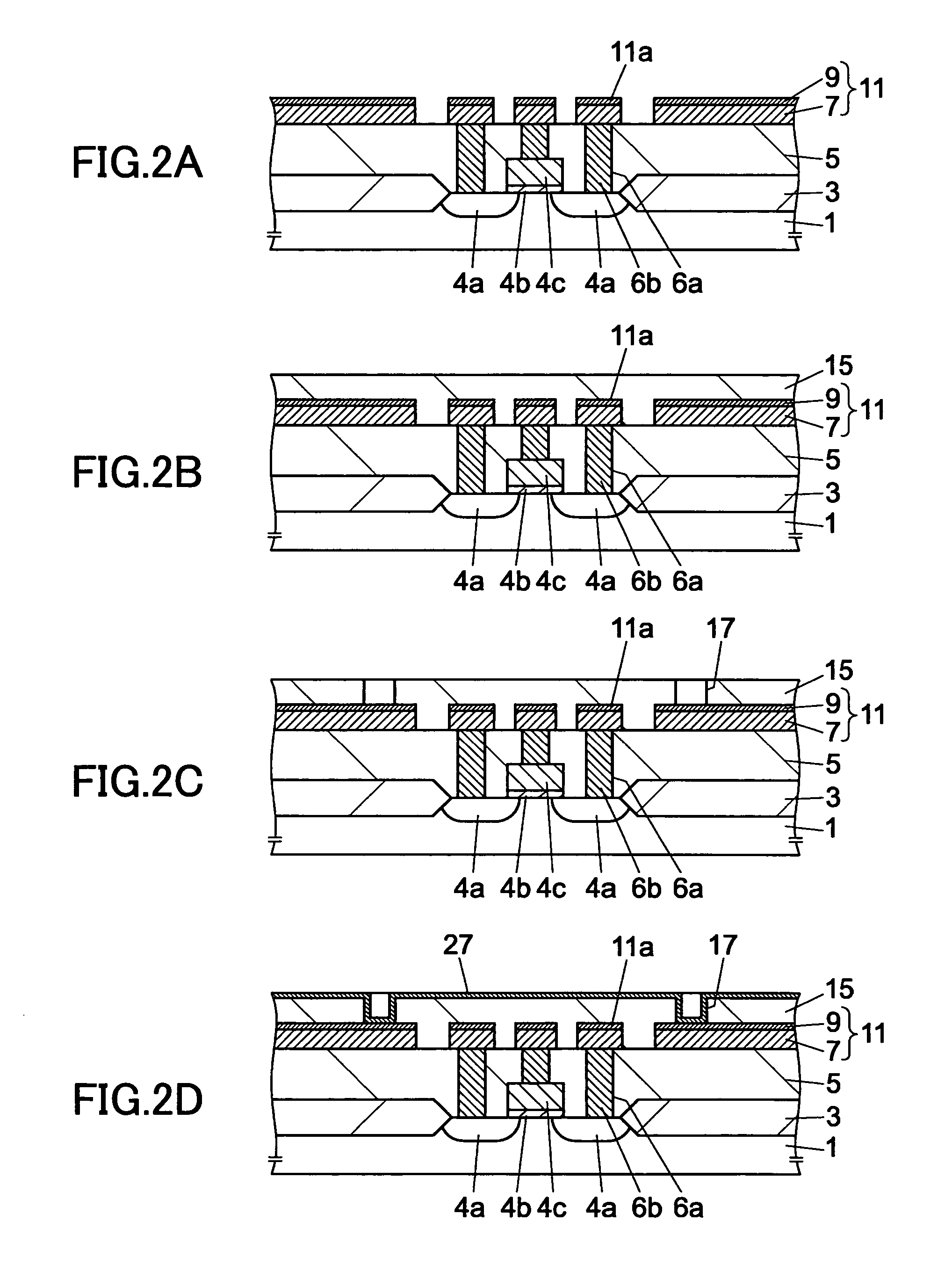
[0045]For example, when an NSG (non-doped silicate glass) film is used as an underground insulator film of a metal thin-film-resistor object, since it is hard to diffuse the metal thin-film-resistor object in the underground insulator film, high laser power is needed when performing a laser trimming process on the metal thin-film-resistor object. Then, a problem arises in that adjacent regions of the metal thin-film-resistor object may be damaged, the adjacent regions including a passivation film formed on the metal thin-film-resistor object, an element under the metal thin-film-resistor object, and a silicon substrate.

SUMMARY OF THE INVENTION

[0046]It is a general object of the present invention to provide a semiconductor device equipped with an integrated circuit including a metal thin-film-resistor object, wherein damage of a region adjacent to the metal thin-film-resistor object by laser irradiation is reduced, substantially obviati...


PUM


Abstract

A semiconductor device equipped with an integrated circuit including a metal thin-film-resistor object is disclosed. The semiconductor device includes a lower layer side insulator film formed on a semiconductor substrate, a metal wiring pattern formed on the lower layer side insulator film, an underground insulator film having a silicon oxide-film that contains at least phosphor, or phosphor and boron in the uppermost layer formed on the lower layer side insulator film and the metal wiring pattern, and a connection hole formed in the underground insulator film on the metal wiring pattern. The metal thin-film-resistor object is formed covering the underground insulator film, and inside of the connection hole, and is electrically connected to the metal wiring pattern in the connection hole.

Description

BACKGROUND OF THE INVENTION[0001]1. Field of the Invention[0002]The present invention generally relates to a semiconductor device, and especially relates to a semiconductor device equipped with an integrated circuit including a metal thin-film-resistor.[0003]2. Description of the Related Art[0004]In an analog integrated circuit, resistors are abundantly used as important components. In recent years and continuing, resistors consisting of a metal thin film (henceforth a metal thin-film-resistor) attract attention in view of low temperature dependency (henceforth TCR) of the resistance. As a material of the metal thin-film-resistors, chromium silicon (CrSi), nickel chromium (NiCr), tantalum nitride (TaN), chromium silicide (CrSi2), chromium silicide nitride (CrSiN), chromium silicon oxy (CrSiO), etc., are used.[0005]It is often the case that the metal thin-film-resistor object of a semiconductor device is formed in the film thickness of less than 100 nm (1000 Å (angstrom)) in order to...

Claims


Application Information

Patent Timeline
Patent Type & Authority Patents(United States)
IPC IPC(8): H01L29/00
CPCH01L21/76831H01L21/76846H01L28/24H01L21/76883H01L27/0629H01L21/76865H01L23/5228H01L21/76805
Inventor KATO, HIDENORIMORI, MASAHIDEWATANABE, HIROFUMI
Owner RICOH KK
Why Eureka
Try Eureka