Method for manufacturing liquid crystal display device

a technology of liquid crystal display and manufacturing method, which is applied in the direction of semiconductor devices, instruments, electrical devices, etc., can solve the problems of large quantity of waste, difficulty in manufacturing a display panel at low cost, and waste of material cost, so as to improve the utilization efficiency of materials and simplify the manufacturing step.

Inactive Publication Date: 2008-10-21
SEMICON ENERGY LAB CO LTD
View PDF94 Cites 24 Cited by
  • Summary
  • Abstract
  • Description
  • Claims
  • Application Information

AI Technical Summary

Benefits of technology

[0005]However, a size of a glass substrate is further enlarged to 1000 mm×1200 mm or 1100 mm×1300 mm in the fifth generation, and a size of 1500 mm×1800 mm or more is assumed in the next generation. Therefore, it becomes difficult to manufacture a display panel at low cost with good productivity by a conventional patterning method. In other words, when a plurality of times of light-exposure treatment is performed by the above-described consecutive light exposure, a processing time is increased and huge investment is required for developing a photolithography apparatus that can treat a large-sized substrate.
[0007]The present invention is made in view of the above situation, and it is an object of the present invention to provide a liquid crystal display device which can be manufactured with utilizing efficiency of a material improved and with a manufacturing step simplified and also a manufacturing technique thereof.
[0020]According to the present invention, a wiring layer or a mask can be directly patterned by a droplet discharge method; therefore, it is possible to obtain a thin film transistor with utilization efficiency of a material improved and with a manufacturing step simplified, and a liquid crystal display device using the thin film transistor.

Problems solved by technology

Therefore, it becomes difficult to manufacture a display panel at low cost with good productivity by a conventional patterning method.
Moreover, a method for forming various types of thin films over an entire surface of a substrate and for removing the thin films with a small region left by etching includes a problem that a material cost is wasted and a large quantity of waste is required to treat.

Method used


Image

  • Method for manufacturing liquid crystal display device
  • Method for manufacturing liquid crystal display device
  • Method for manufacturing liquid crystal display device

Examples


embodiment mode 1

[0070]A method for manufacturing a channel protection type thin film transistor is described in this embodiment mode.

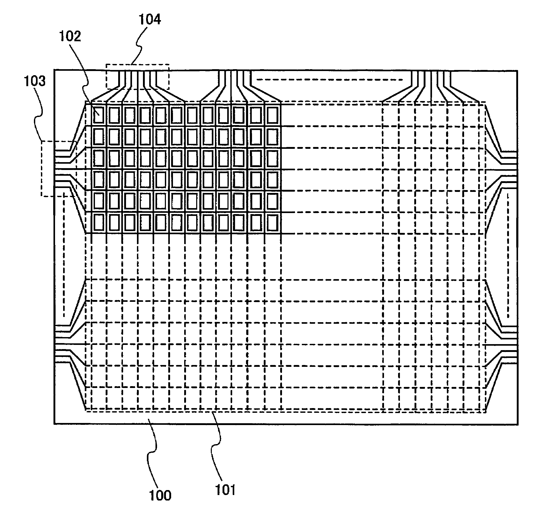
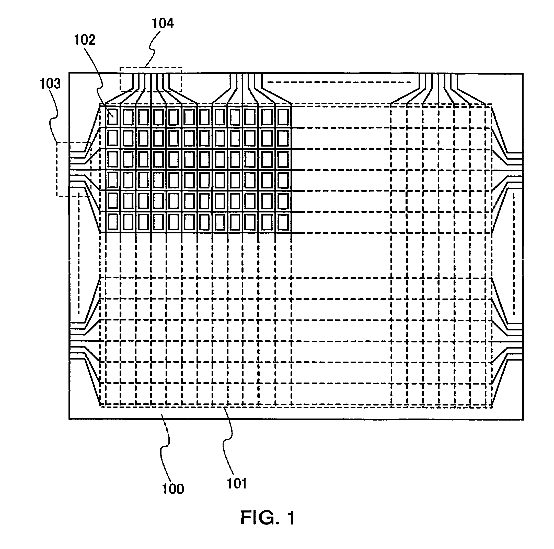
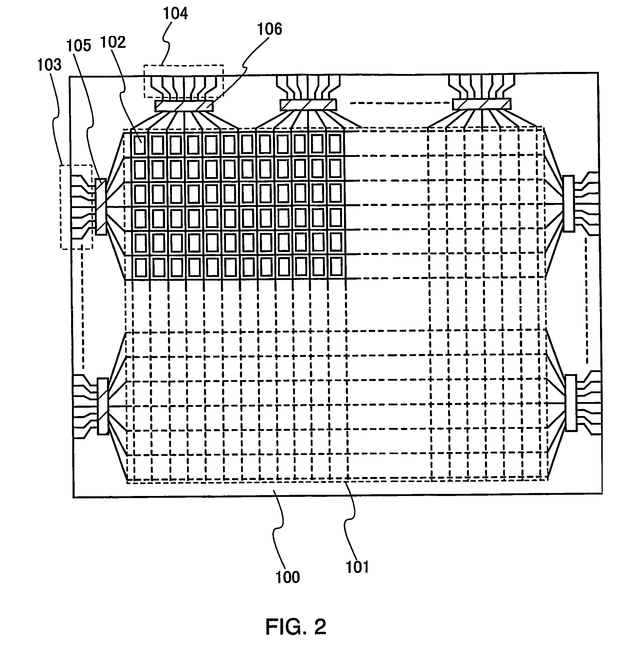
[0071]FIG. 4B shows a step of forming a gate electrode layer and a gate wiring layer which is connected to the gate electrode layer over a substrate 100 by a droplet discharge method. Note that FIG. 4B schematically shows a longitudinal sectional structure, and a planar structure corresponding to a line A-B and a line C-D in FIG. 4B is shown in FIG. 13, which can also be referred to simultaneously.

[0072]In addition to a non-alkaline glass substrate manufactured by a fusion method or a floating method such as barium borosilicate glass, alumino borosilicate glass, or aluminosilicate glass and a ceramic substrate, a plastic substrate having enough heat resistance to withstand a processing temperature of this manufacturing step or the like can be used for the substrate 100. In addition, a semiconductor substrate of single crystal silicon or the like, or a metal substrate ...

embodiment mode 2

[0112]Embodiment Mode 1 shows a structure in which the pixel electrode layer 224 and the source-drain wiring layer 220 are directly in contact with each other; however, an insulating layer may be interposed therebetween as another mode.

[0113]In this case, an insulating layer 240 functioning as a protective film is formed when up to the step show in FIG. 5C is completed (ref. FIG. 8A). A coating of silicon nitride or silicon oxide formed by a sputtering method or a plasma CVD method may be employed as the protective film. It becomes necessary to form an opening 241 in the insulating layer 240, and the source-drain wiring layer 220 is electrically connected to a pixel electrode layer 224 through the opening 241 (ref. FIG. 8B). At the time of forming the opening 241, an opening 242 necessary for attaching a connection terminal later may be simultaneously formed. Reference number 244 denotes an insulating layer.

[0114]A method for forming the openings 241 and 242 is not specifically limi...

embodiment mode 3

[0116]A method for manufacturing a channel etch thin film transistor is described in this embodiment mode.

[0117]A gate wiring layer 202, a gate electrode layer 203, and a capacitor wiring layer 204 are formed over a substrate 100 by discharging a composition including a conductive material with a droplet discharge method. Subsequently, a gate insulating layer is formed to be a single layer or to have a laminated structure by a plasma CVD method or a sputtering method. A specifically preferable mode of the gate insulating layer corresponds to a lamination body of three layers of an insulating layer 208 made of silicon nitride, an insulating layer 209 made of silicon oxide, and an insulating layer 210 made of silicon nitride. Furthermore, up to a semiconductor layer 211 functioning as an active layer is formed. The above-mentioned steps are similar to those in Embodiment Mode 1.

[0118]An n-type semiconductor layer 301 is formed on the semiconductor layer 211 (ref. FIG. 10A). Next, a ma...


PUM


Abstract

A conventionally followed technique of manufacturing a liquid crystal display device is a method for forming various types of coatings over an entire surface of a substrate and for removing the coatings with a small region left by etching, which requires wasting a material cost and treating a large quantity of waste. A liquid crystal display device is manufactured by forming at least one or more of patterns necessary for manufacturing a liquid crystal display device by a method capable of selectively forming a pattern. A droplet discharge method capable of forming a predetermined pattern by selectively discharging a droplet of a composition prepared for a specific purpose is employed as the method capable of selectively forming a pattern.

Description

TECHNICAL FIELD[0001]The present invention relates to a liquid crystal display device including an active element such as a transistor formed over a large-area glass substrate and to a manufacturing method thereof.BACKGROUND ART[0002]Conventionally, a so-called active matrix liquid crystal display panel including a thin film transistor (hereinafter also referred to as a “TFT”) over a glass substrate is manufactured by patterning various thin films through a light-exposure step using a photomask as in a manufacturing technique of a semiconductor integrated circuit.[0003]A production technique for efficiently performing mass-production by cutting a plurality of liquid crystal display panels out of one mother glass substrate has been adopted so far. The size of a mother glass substrate has been enlarged from 300 mm×400 mm of the first generation in the early 1990s to 680 mm×880 mm or 730 mm×920 mm of the fourth generation in 2000. Furthermore, the production technique has progressed so...

Claims


Application Information

Patent Timeline
Patent Type & Authority Patents(United States)
IPC IPC(8): H01L21/00H01L21/336H01L21/77H01L21/84H01L27/12H01L29/423H01L29/786
CPCH01L27/12H01L27/1292H01L29/66765H01L29/42384H01L27/1285H01L29/78696H01L2224/16H01L2224/48091H01L2224/48227H01L2224/48464H01L2924/01029H01L2924/01046H01L2924/01077H01L2924/01078H01L2924/01079H01L2924/04941H01L2924/09701H01L2924/19041H01L2924/3025H01L2924/10253H01L2224/45144H01L2924/00014H01L2924/00H01L2224/04026H01L2224/05568H01L2224/05573H01L2224/2929H01L2224/293H01L2224/83851H01L2224/05599G02F1/136286H01L21/288H01L27/1214H01L27/124
Inventor YAMAZAKI, SHUNPEIMAEKAWA, SHINJINAKAMURA, OSAMU
Owner SEMICON ENERGY LAB CO LTD
Why Eureka
Try Eureka