Magnetic body, magnetic device using the same, and method of manufacturing the same

Inactive Publication Date: 2008-12-30
NIPPON TELEGRAPH & TELEPHONE CORP
View PDF2 Cites 29 Cited by
  • Summary
  • Abstract
  • Description
  • Claims
  • Application Information

AI Technical Summary

Benefits of technology

[0016]The present invention has been completed in view of the above difficulties and has an object to provide a magnetic body, made from non-magnetic material, that allows quantum dot system, surrounded by barrier layers, to be bonded to one anothe

Problems solved by technology

However, in order for a further large number of quantum dots to be bonded to one another to cause ferromagnetism to be generated in the artificial crystal, the quantum dots scaled in the same size must be periodically arranged in a certain particular lattice structure and, hence, an issue ari

Method used


Image

  • Magnetic body, magnetic device using the same, and method of manufacturing the same
  • Magnetic body, magnetic device using the same, and method of manufacturing the same
  • Magnetic body, magnetic device using the same, and method of manufacturing the same

Examples


first embodiment

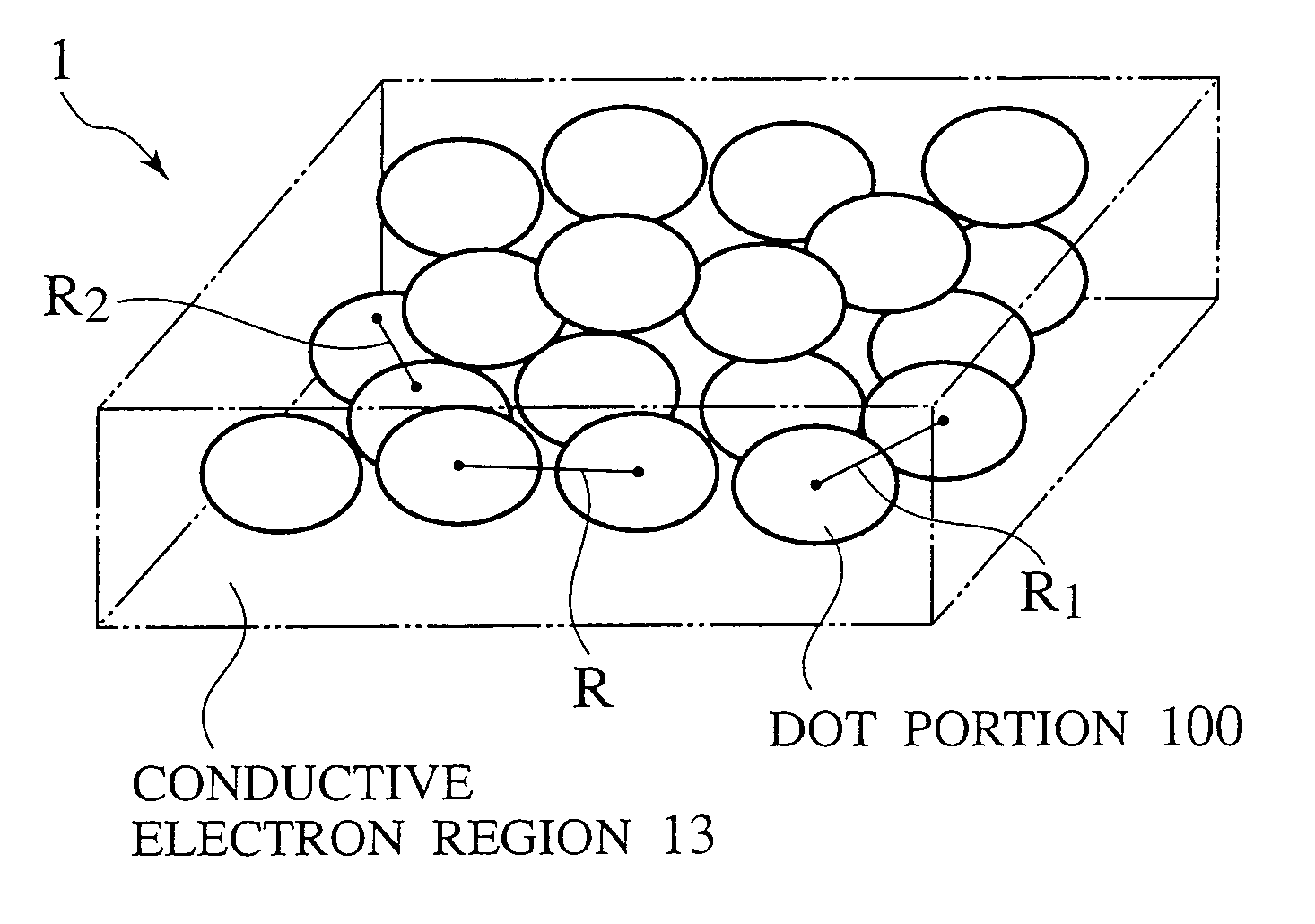
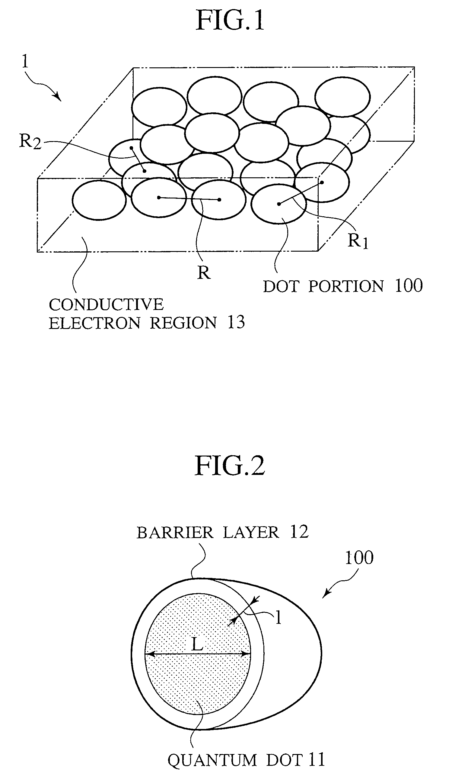
[0090]FIG. 1 is an illustrative view showing a structure of a magnetic body of a first embodiment of the present invention. Further, FIG. 2 is an illustrative view showing a structure of a dot portion 100 of FIG. 1. As shown in these figures, a magnetic body 1 has a structure in that a plurality of quantum dots 11, which forms a localized electron region having a localized spin, in which at least one electron is confined, are buried intervening the dot portion 100, surrounded by a barrier layer (a barrier potential region) 12 by which the electron is confined in each quantum dot 11, in a conductive electron region 13, composed of a conductive electron system, which has a lower energy than that of the barrier layer 12.

[0091]Also, it is not objectionable for magnitudes of energies of the quantum dots 11 of the electron localized region and the conductive electron region 13 to lie at arbitrarily values.

[0092]Further, the relationships among the quantum dot 11, the barrier layer 12 and ...

second embodiment

[0116]FIG. 6 is an illustrative view showing a structure of a magnetic body of a second embodiment of the present invention. The magnetic body 5 shown in FIG. 6 contemplates the use of two-dimensional conductive electron gas formed in a two-dimensional electron system interface 56 such as a hetero interface of a compound semiconductor composed of GaAs and aluminum-gallium-arsenate (AlGaAs), and an inverted layer of a silicon MOS (Metal Oxide Semiconductor) transistor composed of silicon and silicon dioxide.

[0117]While FIG. 6 shows that the two-dimensional electron system interface 56 is formed at a boundary between a semiconductor 54 and a semiconductor 55, in a case where this two-dimensional electron system interface 56 includes the hetero interface of the compound semiconductor set forth above, the semiconductor 54 is composed of GaAs and the semiconductor 55 the insulation layer) is composed of AlGaAs. In this case, GaAs and AlGaAs may also be reversed. Also, in case of the two-...

third embodiment

[0124]FIG. 8 is an illustrative view showing a structure of a magnetic body of a third embodiment of the present invention. The magnetic body 6 shown in this figure is manufactured applying an etching process method or a selective growing method to a semiconductor. More particularly, when processing a semiconductor to cut out a portion thereof by an etching process to finally form a configuration shown in FIG. 8, electrons transfer depending upon this configuration to allow the electrons to accumulate in a quantum this wire region with its cross section represented in a substantially rhombus shape in the same figure, thereby forming the quantum dot portions 61. Also, the size of the quantum dot region 61 substantially equals the sizes of the quantum dot portions of the first and second embodiments. Further, while in FIG. 8, the cross sectional areas of all the quantum dots 61 that are formed have been shown and described in the substantially same rhombus shape, it is of course to be...


PUM


Abstract

A magnetic body composed of non-magnetic material, includes a plurality of localized electron regions in each of which at least one electron is confined to form a localized spin, a barrier potential region having a higher energy than a Fermi energy of an electron in the localized electron region and permitting an electron to be confined in the respective localized electron regions, and a conductive electron region including a conductive electron system having a lower energy than an energy of the barrier potential region, wherein the respective localized electron regions are disposed separate from one another via the barrier potential region and the conductive electron region.

Description

CROSS REFERENCE TO RELATED APPLICATION[0001]This application claims benefit of priority under 35 U. S. C. § 119 to Japanese Patent Application No. 2002-256036, filed on Aug. 30, 2002, the entire contents of which are incorporated by reference herein.BACKGROUND OF THE INVENTION[0002]1. Field of the Invention[0003]The present invention relates to a magnetic body, a magnetic device using the same, and a method of manufacturing the same.[0004]2. Description of the Related Art[0005]Conventionally, magnetic memory media and magnetic sensors have been produced from magnetic bodies made from magnetic materials such as natural magnets (e.g., magnetite: Fe3O4), alloy magnets (e.g., chrome steel and high cobalt steel), magnets composed of alnico, ferrite and a rare earthes, and more.[0006]Since all of these magnetic materials include magnetic metals, production processes of these magnetic materials, e.g., manufacturing process of a magnetic device on an LSI (Large Scale Integration) substrate ...

Claims


Application Information

Patent Timeline
IPC IPC(8): H01L29/06H01F1/00H01F10/00
CPCB82Y25/00H01F1/009H01F10/007H01F1/404H01F10/193H01F41/302Y10S977/932
Inventor TAMURA, HIROYUKITAKAYANAGI, HIDEAKI
Owner NIPPON TELEGRAPH & TELEPHONE CORP
Why Eureka
Try Eureka