Arsenic and phosphorus doped silicon wafer substrates having intrinsic gettering

a technology of arsenic and phosphorus, which is applied in the field of silicon wafer preparation, can solve the problems of affecting the operation of the device, contaminating molten silicon with various impurities, and precipitating harmful or beneficial effects, and achieves greater wafer-to-wafer uniformity and low resistivity

Active Publication Date: 2009-02-03
GLOBALWAFERS CO LTD
View PDF83 Cites 21 Cited by
  • Summary
  • Abstract
  • Description
  • Claims
  • Application Information

AI Technical Summary

Benefits of technology

[0006]Among the various aspects of the present invention, therefore, is the provision of low resistivity (N+ / N++), arsenic or phosphorous doped single crystal silicon wafers, which, during the heat treatment cycles of essentially any electronic device manufacturing process, reliably forms oxygen precipitates, and a process for their preparation. Advantageously, this process yields wafers having greater wafer-to-wafer uniformity and, in addition, relaxes certain single crystal growth constraints required by certain prior approaches.
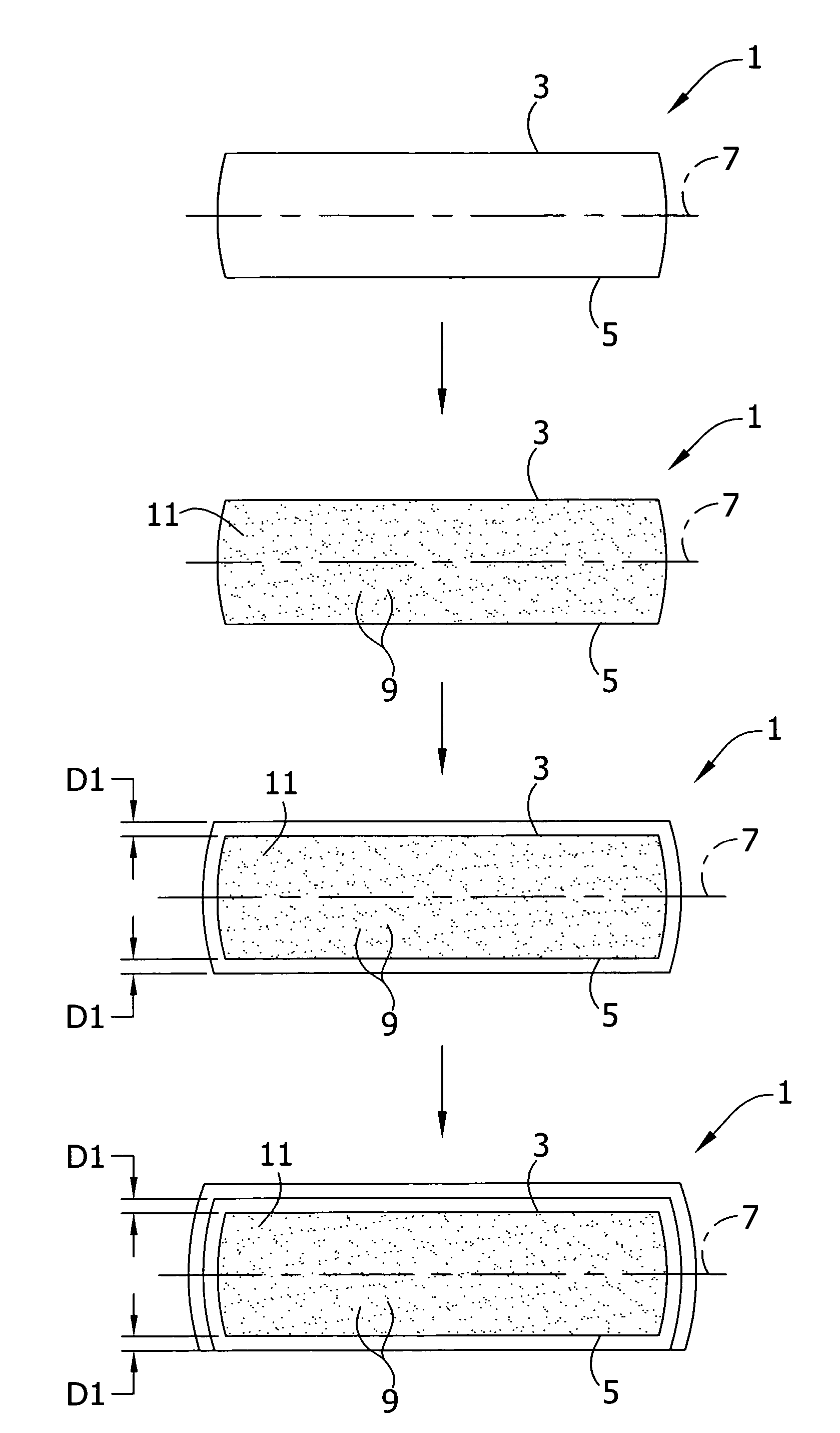
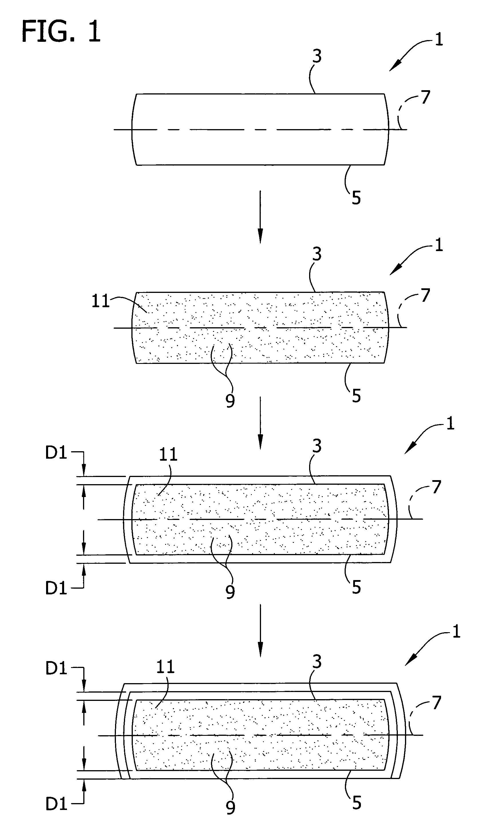
[0007]Briefly, therefore, the present invention is directed to a wafer sliced from a single crystal silicon ingot grown by the Czochralski method comprising a front surface, a back surface, an imaginary central plane between the front and back surfaces, a front surface layer which comprises a first region of the wafer between the front surface and a distance, D1, measured from the front surface and toward the central plane, and a bulk layer which comprises a second region of the wafer between the central plane and the first region. The wafer has a resistivity of less than 5 mΩ-cm, is doped with phosphorous or arsenic, and has a supersaturated concentration of crystal lattice vacancies in the bulk layer whereby (a) oxygen precipitates form in the bulk layer at a concentration of at least 1×10⁷ oxygen precipitates / cm3 upon subjecting the wafer to an oxygen precipitation heat-treatment at a temperature in excess of 700° C., and (b) the supersaturated concentration of crystal lattice vacancies is reduced and the formation of oxygen precipitates in the bulk layer at a concentration of at least 1×10⁷ oxygen precipitates / cm3 is avoided by (i) heating the wafer to an annealing temperature of at least 950° C. at a rate of at least 2° C. / sec, and (ii) cooling the wafer from the annealing temperature to 700° C. or less before the wafer is subjected to an oxygen precipitation heat-treatment at a temperature in excess of 700° C.

Problems solved by technology

Molten silicon is contaminated with various impurities, among which is mainly oxygen, during the time it is contained in a quartz crucible.
Depending upon their location in the wafer, the precipitates can be harmful or beneficial.
Oxygen precipitates located in the active device region of the wafer can impair the operation of the device.
Such wafers have presented challenges.
This approach, however, was not entirely satisfactory.
Also, this approach requires carbon concentration to increase as a function of ingot length; resulting in a lack of wafer-to-wafer uniformity and more complex crystal growth process control.

Method used


Image

  • Arsenic and phosphorus doped silicon wafer substrates having intrinsic gettering
  • Arsenic and phosphorus doped silicon wafer substrates having intrinsic gettering

Examples


example

[0048]Red phosphorus doped silicon single crystals were pulled by the Czochralski method, sliced and polished to form silicon wafers. The initial oxygen concentration of each wafer was from about 12 PPMA to about 18 PPMA, and the resistivity was from about 1.2 mΩ-cm to about 1.7 mΩ-cm. The wafers were then subjected to rapid thermal annealing in nitrogen, rapidly cooled, and subjected to oxygen precipitate stabilization and growth. The temperature of the rapid thermal anneal was varied as shown in TABLE I, but all samples were annealed for 15 seconds. The samples were cooled at 60° C. / sec. Oxygen precipitate formation and stabilization occurred at 800° C. temperature for 4 hours, followed by 1000° C. for 16 hours. The average concentration and peak concentration of oxygen precipitates were measured at the center, at half the radius, and at the edge of each wafer. It was observed that for all samples the peak concentration occurred near the wafer surface. The results are depicted in ...


PUM

PropertyMeasurementUnit
temperatureaaaaaaaaaa
diameteraaaaaaaaaa

Abstract

A process for the preparation of low resistivity arsensic or phosphorous doped (N+ / N++) silicon wafers which, during the heat treatment cycles of essentially any arbitrary electronic device manufacturing process, reliably form oxygen precipitates.

Description

FIELD OF THE INVENTION[0001]The present invention generally relates to the preparation of silicon wafers used in the manufacture of electronic components. More particularly, the present invention relates to a process for the preparation of low resistivity arsenic or phosphorous doped (N+ / N++) silicon wafers which, during the heat treatment cycles of essentially any arbitrary electronic device manufacturing process, reliably form oxygen precipitates.BACKGROUND OF THE INVENTION[0002]Single crystal silicon, which is the starting material for most processes for the fabrication of semiconductor electronic components, is commonly prepared with the so-called Czochralski (Cz) process wherein a single seed crystal is immersed into molten silicon and then grown by slow extraction. Molten silicon is contaminated with various impurities, among which is mainly oxygen, during the time it is contained in a quartz crucible. At the temperature of the silicon molten mass, oxygen comes into the crysta...

Claims


Application Information

Patent Timeline
Patent Type & Authority Patents(United States)
IPC IPC(8): H01L27/01H01L27/12H01L31/0392
CPCC30B29/06C30B33/02H01L21/3225H01L21/20
Inventor FALSTER, ROBERT J.VORONKOV, VLADIMIRBORIONETTI, GABRIELLA
Owner GLOBALWAFERS CO LTD
Why Eureka
Try Eureka