
Capacitive devices, organic dielectric laminates, and printed wiring boards incorporating such devices, and methods of making thereof

a technology of organic dielectric laminates and capacitors, applied in the direction of fixed capacitors, solid-state devices, synthetic resin-layered products, etc., can solve the problems of limiting the capability of the final capacitor, limiting the dielectric constant of the dielectric layer, and regarding certain electrical properties, etc., to achieve low leakage current, high dielectric withstanding voltage, and desirable electrical and physical properties

Active Publication Date: 2009-02-24
DUPONT ELECTRONICS INC
View PDF19 Cites 19 Cited by
  • Summary
  • Abstract
  • Description
  • Claims
  • Application Information

AI Technical Summary

Benefits of technology

The present invention provides dielectric compositions and films for use in capacitor formation in electronic components that have desirable electrical and physical properties, such as high dielectric withstanding voltage and low leakage current. These dielectric compositions and films are especially useful in embedded passive applications. The invention relates to dielectric composites comprising a paraelectric filler and polymeric material where the combination has a dielectric constant between 50 and 150. The invention also relates to the composition above wherein the composition has been processed to form a film and a capacitor comprising the film. The capacitors constructed utilizing the composition of the present invention generally have high capacitance densities and other desirable electrical and physical properties. The invention provides an improved solution for embedded passive applications in printed wiring boards and integrated circuit substrates.

Problems solved by technology

However, the dielectric constant of the dielectric layer is limited and problems exist in regard to certain electrical properties, such as low dielectric withstanding voltage and high leakage current.
Both of these problems limit the capability of the final capacitor and, in many cases, limit the ability to decrease the thickness of the dielectric layer within the capacitor to the desired level.

Method used


Image

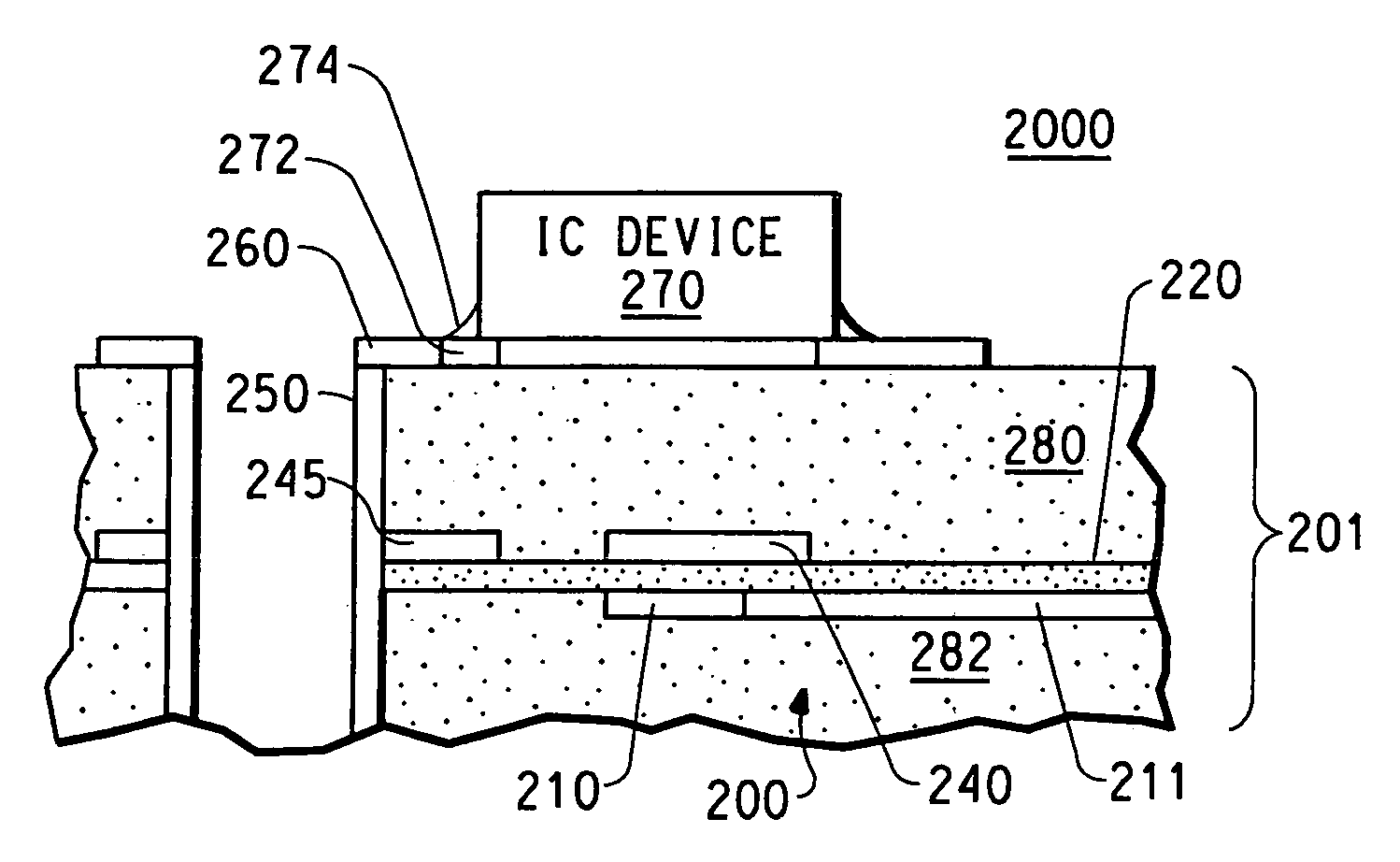
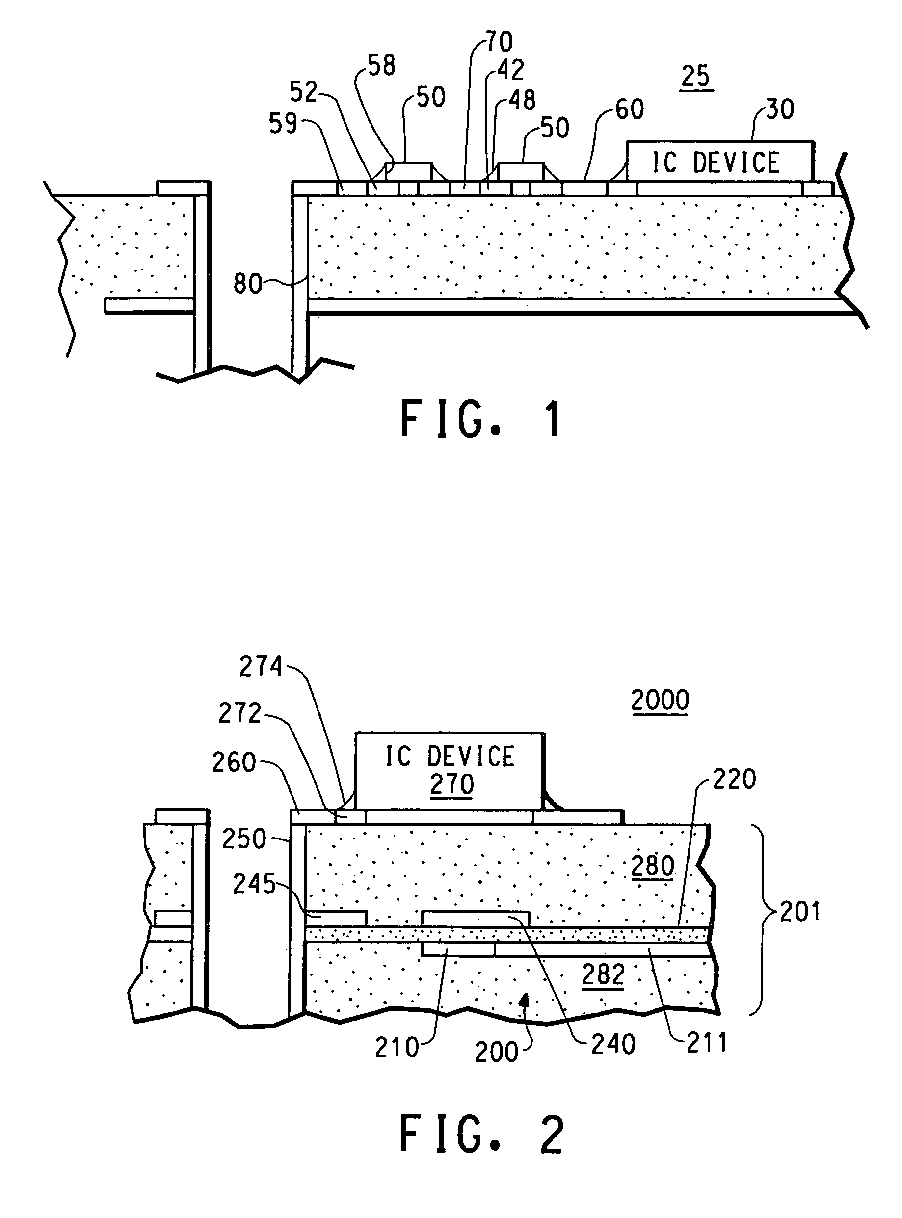
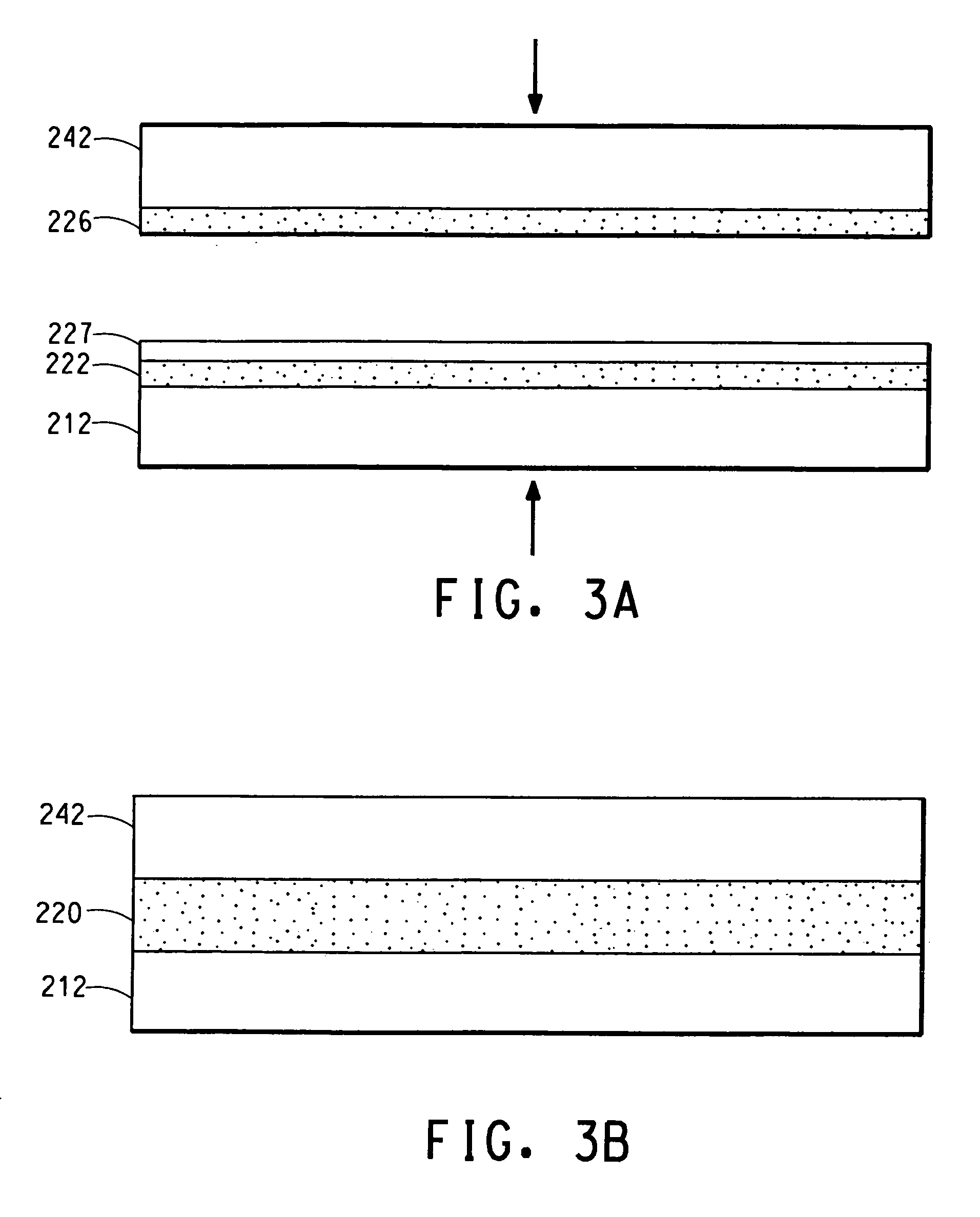
  • Capacitive devices, organic dielectric laminates, and printed wiring boards incorporating such devices, and methods of making thereof
  • Capacitive devices, organic dielectric laminates, and printed wiring boards incorporating such devices, and methods of making thereof
  • Capacitive devices, organic dielectric laminates, and printed wiring boards incorporating such devices, and methods of making thereof

Examples


example 1

[0044]A solution of 160 grams of a polyamic acid derived from the following monomers: pyromellitic dianhydride (PMDA), 4,4′-oxydiphthalic anydride (ODPA) and 1,3-bis-(4-aminophenoxy) benzene (APB-134) was mixed with 120 grams of Dimethylacetamide (DMAC) solvent and 30 grams of DuPont Ti-Pure® R-101 titanium dioxide powder. This solution was stirred in a high speed mixer until the powder was dispersed. Small amounts of additional monomer were added until a viscosity of 500 poise was reached. This solution was then coated on solid surface as a uniform coating. The coating was then dried at 170° C. to remove about 70 to 80% of the solvent. The formed film was then removed from the solid surface. This film was then cured in an oven at 350° C. for 1 hour. The final film thickness was 1.1 mils and the filler loading was 26 volume percent.

[0045]The cured titanium dioxide filled film was then laminated between two sheets of copper foil. Each copper sheet was 36 microns thick. The lamination...

example 2

[0047]A solution of 18 lbs of DMAC and 18 lbs of DuPont Ti-Pure® R-101 titanium dioxide powder was stirred for 1 hour in a high-speed mixer. Then 84 lbs of a polyamic acid derived from the following monomers: pyromellitic dianhydride (PMDA), 4,4′-oxydiphthalic anydride (ODPA) and 1,3-bis-(4-aminophenoxy) benzene (APB-134) was added. This mixture was stirred for an additional 30 minutes. Small amounts of additional monomer were added until a viscosity of 400 poise was reached.

[0048]This solution was then cast on to a continued sheet of copper foil (36 microns thick). The solution was dried at 190° C. to about 90% solids. The coated copper was then cured in an oven at 350° C. for 1 hour. The final film thicknesses were 8 and 12 microns. The filler loading was 29 volume percent.

[0049]The filled polyimide film coated on copper was then laminated to a sheet of copper foil. The copper sheet was 35 microns thick. The lamination used an autoclave under vacuum with maximum lamination tempera...


PUM

PropertyMeasurementUnit
dielectric constantaaaaaaaaaa
volume percentaaaaaaaaaa
particle sizeaaaaaaaaaa

Abstract

A polymeric dielectric composition is disclosed, having a paraelectric filler with a dielectric constant between 50 and 150. Such compositions are well suited for electronic circuitry, such as, multilayer printed circuits, flexible circuits, semiconductor packaging and buried film capacitors.

Description

BACKGROUND INFORMATION[0001]1. Field of the Disclosure[0002]The technical field relates to dielectric composition(s) and film(s) and their use in electronic circuitry and components, such as, multilayer printed circuits, flexible circuits, semiconductor packaging and buried film capacitors.[0003]2. Description of Related Art[0004]An increasing need exists for reducing the size and increasing the performance of integrated circuit components. One common part of the integrated circuit components, for example planar capacitor components, includes a dielectric layer that is formed from a composition comprising a dielectric functional filler material and a polymer. Typically, using a dielectric functional filler material having a high dielectric constant, K, in a capacitor allows for storage of the same amount of electrical charge for a given thickness of the dielectric layer in a reduced capacitor area versus that containing no filler.[0005]Various types of dielectric layers are currentl...

Claims


Application Information

Patent Timeline
Patent Type & Authority Patents(United States)
IPC IPC(8): H01G4/06B32B7/025
CPCB32B7/02B32B15/08B32B15/082B32B15/092B32B15/095B32B15/20B32B27/20B32B27/281B32B27/308C08K3/22H01B3/30H01G4/206H01L23/49894H01L27/016H01L28/55H05K1/162B32B2250/40B32B2264/102B32B2264/12B32B2307/20B32B2307/202B32B2307/204B32B2457/08B32B2457/14B32B2457/16H01L2924/3011H05K2201/0209H05K2201/0355H05K2201/09309H01L2224/32225H01L2924/19105B32B7/025
Inventor COX, G. SIDNEY
Owner DUPONT ELECTRONICS INC
Learn More