Formation of nanowhiskers on a substrate of dissimilar material

a technology of dissimilar materials and nanowhiskers, which is applied in the direction of crystal growth process, polycrystalline material growth, chemically reactive gas growth, etc., can solve the problems of large thermal expansion coefficient difference, defective material, and formation of anti-phase domain walls, so as to achieve high-reliability photonics devices, effective implementation of optical interconnections, and the effect of essentially constant luminescence properties of segments

Inactive Publication Date: 2009-05-05
QUNANO
View PDF67 Cites 31 Cited by
  • Summary
  • Abstract
  • Description
  • Claims
  • Application Information

AI Technical Summary

Benefits of technology

[0035]In a currently preferred embodiment, however, the entire substrate surface is processed towards an ideal condition, followed by deposition on the surface of catalytic particles by an aerosol process. To this end, it is preferred to passivate the surface by means of etching with an acid such as HF. This has the effect that free or dangling bonds on the substrate surface are terminated with hydrogen ions. This prevents further oxide growth on the substrate surface, and maintains ideal surface conditions while aerosol deposition takes place. Aerosol deposition, and any further processing on the substrate surface takes place in accordance with the invention before any significant degradation of the passivation properties of the hydrogen termination. In practice, a time period of about 2 hours may be permissible.
[0044]It will be appreciated that with the present invention, structures and processes that have been previously proposed and demonstrated (for example, in the aforementioned U.S. patent application Ser. No. 10 / 613,071, published as No. 2004-0075464, and International Patent Application Publication No. WO-A-04 / 004927) may be more accurately and reliably implemented. In particular, the processes disclosed for forming epitaxial layers on silicon substrates may be implemented with a reduced risk of non-epitaxial growth.
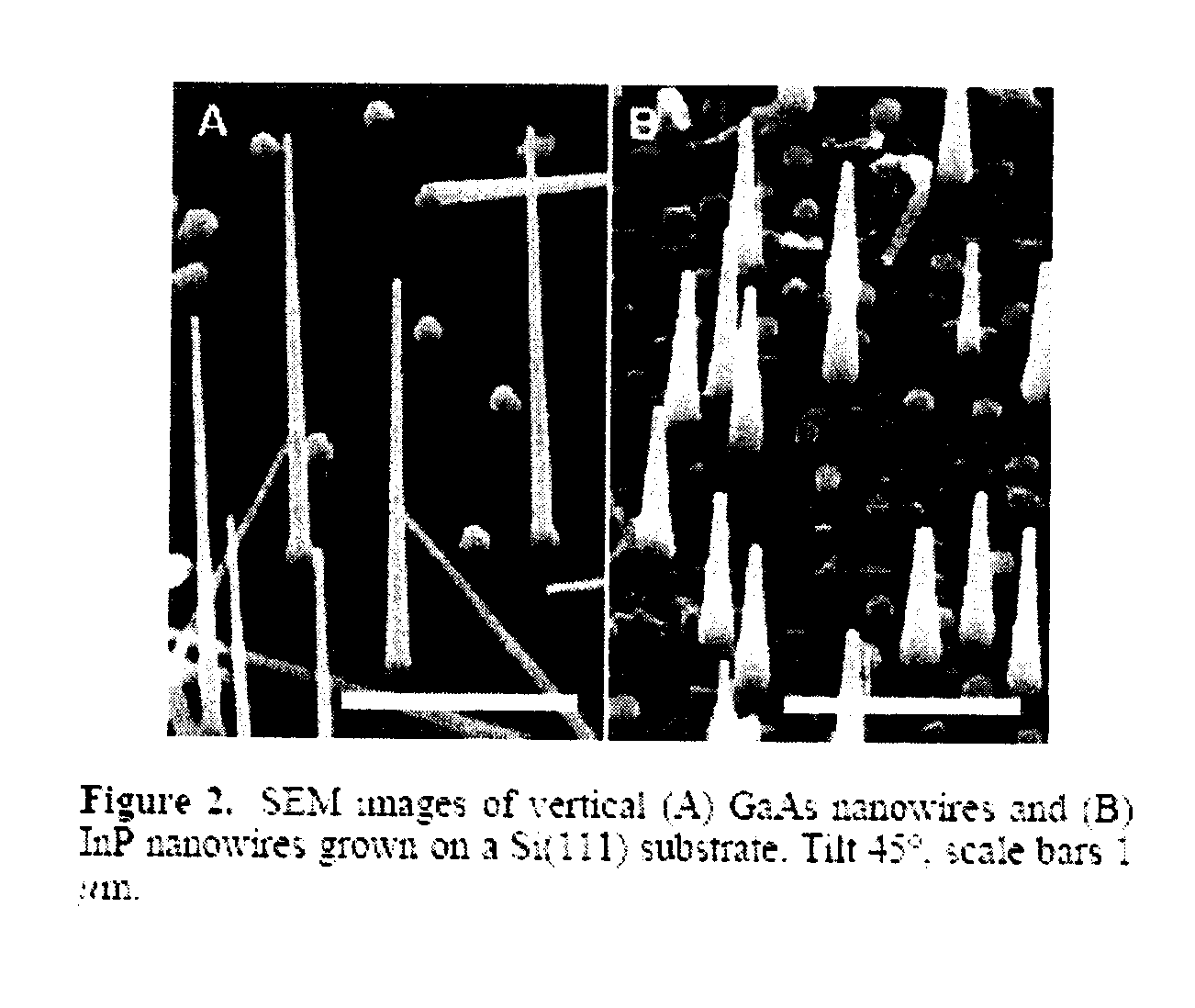
[0058]In a further aspect, the invention permits the incorporation of double heterostructure segments in such nanowhiskers, allowing efficient room-temperature generation of light from, e.g., III-V nanowires grown on Si substrates. Advanced heterostructure devices presently realized on very expensive, silicon-incompatible III-V substrates, such as resonant tunnelling diodes, superlattice device structures and heterostructure photonic devices for on-chip communication, are, in accordance with the invention, available as complementary device technologies for integration with silicon.
[0060]It has been found that such heterojunctions may be very precisely and accurately formed with sharp or abrupt junctions extending over only a few atomic lattice planes. The material of the nanowhisker in general is single crystal, single domain, pure epitaxial growth without defect or dislocation. It has been found that the optical characteristics of such nanowhiskers are very high quality, with the luminescence properties remaining constant from very low cryogenic temperatures up to room temperatures, without quenching of the luminescence. This arises, in significant part, because the confining potential of the quantum well formed by the heterojunctions bounding the segment is well defined (at least 200 meV up to 500 meV) and much greater than the thermal energy at room temperature, kT (˜25 meV), so that the thermal movement of free charge carriers does not disturb the energy distributions of the carriers within the quantum well.
[0062]Further, the luminescence properties of the segment remain essentially constant, with substantially no quenching, from cryogenic temperatures up to room temperature, thereby providing for highly reliable photonics devices. In accordance with the invention, the provision of nanowhiskers containing optically active material on a silicon substrate permits a very effective implementation of optical interconnects on a silicon chip. As processor speeds increase, a limiting factor in silicon chips is speed of transmission of optical pulses along buses formed as conductive lines on the substrate. A means of avoiding this limitation is to provide a data bus in the form of an optical interconnect comprising an optical path including a light emitter and a light receiver positioned on the substrate surface.

Problems solved by technology

Epitaxial growth of III-V semiconductors on Si presents a number of difficulties, such as lattice mismatch, differences in crystal structure (III-V's have a polar zinc blende or wurtzite structure whereas Si has a covalent diamond structure), and a large difference in thermal expansion coefficient.
A major challenge has been to avoid the formation of antiphase domains related to the initiation of III-V growth on two atomic planes of silicon differing by one atomic layer, which leads to the formation of anti-phase domain walls and defective material.

Method used


Image

  • Formation of nanowhiskers on a substrate of dissimilar material
  • Formation of nanowhiskers on a substrate of dissimilar material
  • Formation of nanowhiskers on a substrate of dissimilar material

Examples


examples

[0076]Starting material was “Toyo” Epitaxial Silicon Wafers, P type substrate with a P type epilayer orientation (111).

[0077]

DopantResistivityThicknessSubstrateBoronΩ cm245 μmLayerBoron12Ω cm 27 μm

[0078]Preparation Prior to Growth

[0079]1) Clean with ultrasonic Tri-clean to remove organic residues and particles.

[0080]The wafer was placed in a test tube and solution a) below was added. The test tube was put in ultrasonic bath at 35 KHz for 2-3 minutes. After, the bath the solution was decanted and the next solution was added. The process repeated for solutions b)-d) in that order.

[0081]a) Trichloroethylene (proanalysi)

[0082]b) Acetone (proanalysi)

[0083]c) Ethanol (95%)

[0084]d) Milli-Q-H2O

[0085]The water was decanted and refilled 2-3 times in Milli-Q-H2O (18.2 W cm 25° C.). Rinse the wafer.)

[0086]2) The wafer was removed from the rinse water and immediately cleaned with Piranha Etch to remove any remaining organic residues.

[0087]The following were measured and mixed in a separate conta...


PUM

PropertyMeasurementUnit
thicknessaaaaaaaaaa
sizeaaaaaaaaaa
time periodaaaaaaaaaa

Abstract

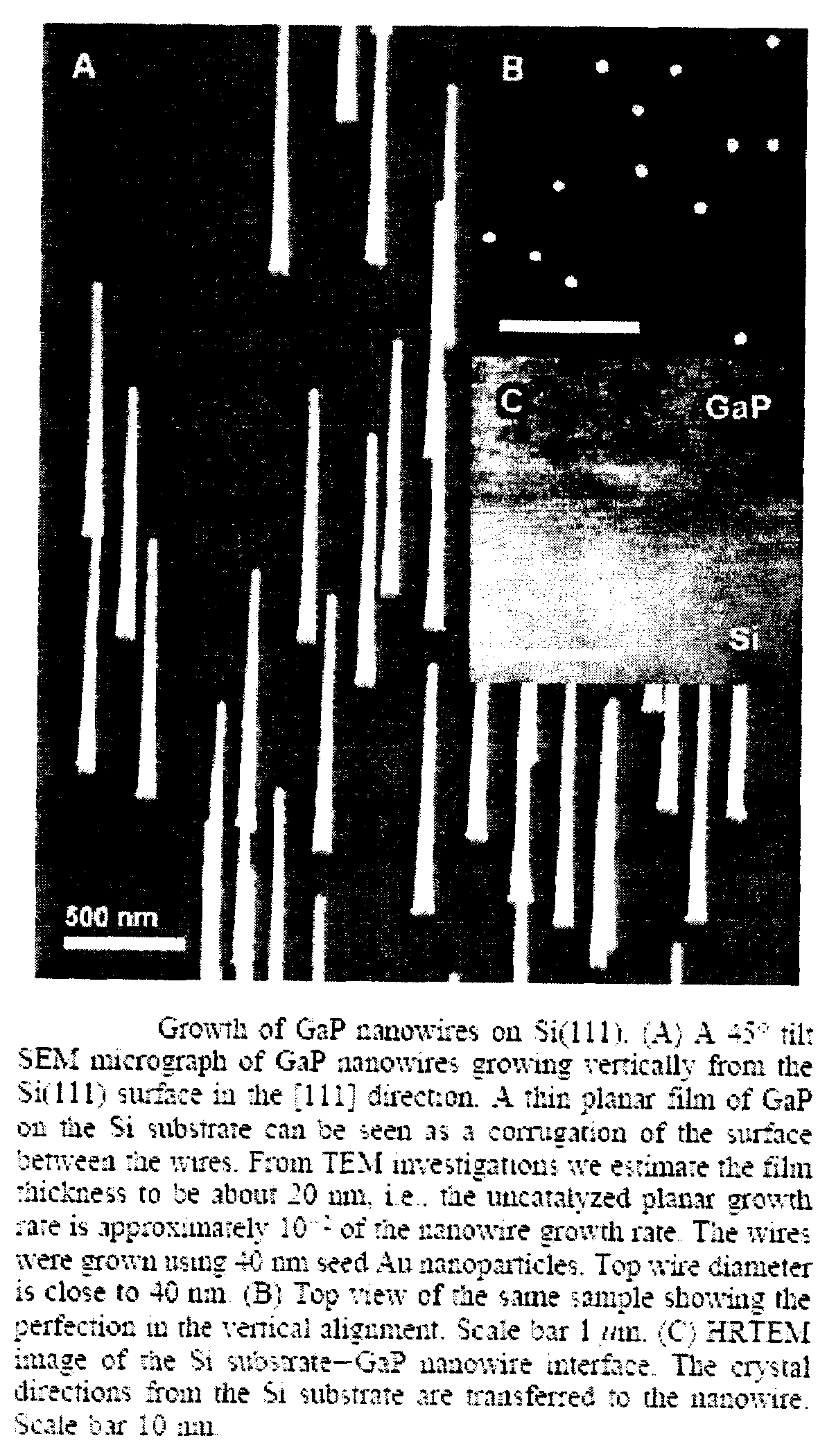
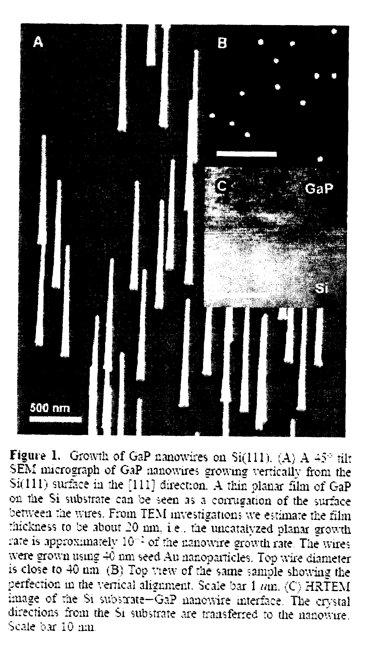
A method for forming a nanowhisker of, e.g., a III-V semiconductor material on a silicon substrate, comprises: preparing a surface of the silicon substrate with measures including passivating the substrate surface by HF etching, so that the substrate surface is essentially atomically flat. Catalytic particles on the substrate surface are deposited from an aerosol; the substrate is annealed; and gases for a MOVPE process are introduced into the atmosphere surrounding the substrate, so that nanowhiskers are grown by the VLS mechanism. In the grown nanowhisker, the crystal directions of the substrate are transferred to the epitaxial crystal planes at the base of the nanowhisker and adjacent the substrate surface. A segment of an optically active material may be formed within the nanowhisker and bounded by heterojunctions so as to create a quantum well wherein the height of the quantum well is much greater than the thermal energy at room temperature, whereby the luminescence properties of the segment remain constant without quenching from cryogenic temperatures up to room temperature.

Description

CROSS-REFERENCE TO RELATED APPLICATIONS[0001]This application claims the benefit of the priority of U.S. Provisional Patent Application No. 60 / 582,513, filed Jun. 25, 2004, the entirety of which is incorporated herein by reference.BACKGROUND OF THE INVENTION[0002]1. Field of the Invention[0003]This invention relates generally to structures produced by techniques of nanotechnology, and methods of producing such structures.[0004]More specifically, the invention relates to such structures and devices incorporating at least one element, essentially in one-dimensional form, which is of nanometer dimensions in its width or diameter, which is produced with the aid of a catalytic particle, and which is commonly termed a “nanowhisker.”[0005]The invention relates also to a method of forming a nanowhisker of a certain material on a substrate of a dissimilar material.[0006]2. Brief Description of the Prior Art[0007]Nanotechnology covers various fields, including that of nanoengineering, which m...

Claims


Application Information

Patent Timeline
Patent Type & Authority Patents(United States)
IPC IPC(8): H01L21/205
CPCC30B11/12C30B25/005C30B29/40C30B29/48C30B29/60C30B29/605H01L21/02381H01L21/02543H01L21/02546H01L21/02603H01L21/0262H01L21/02639H01L33/0066B82Y30/00H01L21/02551H01L21/02645Y10S977/89Y10S977/762Y10S977/891Y10S977/815
Inventor SAMUELSON, LARS IVARMARTENSSON, THOMAS M. I.
Owner QUNANO
Why Eureka
Try Eureka