Phase-change memory device using Sb-Se metal alloy and method of fabricating the same

a phase-change memory and metal alloy technology, applied in the direction of semiconductor devices, basic electric elements, electrical appliances, etc., can solve the problems of large energy consumption of dram, insignificant power consumption of refresh process, and increase in power consumption, so as to achieve high crystallization speed, low melting point, and high speed

Active Publication Date: 2009-06-16
ELECTRONICS & TELECOMM RES INST
View PDF12 Cites 21 Cited by
  • Summary
  • Abstract
  • Description
  • Claims
  • Application Information

AI Technical Summary

Benefits of technology

[0023]The present invention provides a phase change nonvolatile memory device that can operate at a high speed with a low power consumption and is fabricated using a phase-change material having a low melting point and a high crystallization speed.
[0024]The present invention also provides a method of fabricating a phase change nonvolatile memory device that can operate at a high speed with a low power consumption and is fabricated using a phase-change material having a low melting point and a high crystallization speed.
[0033]The present invention provides a method of fabricating a phase-change memory device using a phase-change material having a low melting point and a high crystallization speed, giving the phase-change memory device a high speed and a low power consumption. The present invention provides a method of fabricating a phase-change memory device using a metal alloy of antimony and selenium as a phase-change material. The phase-change material composed of the metal alloy ensures the phase-change memory device to more reliably operate than a conventional GST material.

Problems solved by technology

When the integration density of a memory device is low, the power consumption of the refresh process is insignificant.
However, as the integration density becomes higher, the power consumption also increases greatly.
For example, at a refresh rate of 1˜10 ms / Mbit, the DRAM consumes a great quantity of energy.
The refresh process of a 1 Gbit DRAM is responsible for most of the device's total power consumption.
However, DRAM memory modules are widely used, because their high power consumption is offset by high speed and competitive price.
However, flash memory is slow and uses a relatively high voltage.
These problems limit the use of flash memory to mobile devices such as digital cameras and mobile phones.
Although flash memory has low reliability in re-writing performance, the number of re-writing operations can be set to be smaller when flash memory is used in a mobile device such as a personal digital assistant.
However, such a reliability of flash memory in re-writing in a mobile device does not ensure stable operation in a general-purpose PC.
However, this method is expensive and greatly increases the size of the memory chip.
However, a semiconductor memory device having all of these characteristics has not yet been commercially produced.
Magneto-resistive RAM (MRAM) devices and ferroelectric RAM (FRAM) device are competition to PRAM devices, but have the problems of difficult manufacturing process and miniaturization.
As described above, since the PRAM device is driven by applying a current to a resistor and using the joule heat to change the crystal structure of a phase-change material, power consumption is likely to be high.
That is, when a PRAM device is fabricated using a conventional larger-semiconductor device manufacturing process, excessive power and heat that the entire system cannot withstand are generated, thereby making it impossible to realize a practical memory device.
In the low power device, the power consumption of a phase-change memory array is low.
Especially, in a highly-integrated memory array where cells are very closed spaced, the heat generated by the operation of a particular memory cell may act as noise and interrupt the memory operation of an adjacent cell.
However, even though the heat generated in the contact portion can be reduced by minimizing the phase change region as in the second method described above, if the generated heat energy cannot be efficiently utilized, a relatively large amount of current has to be applied.
FRAM or MRAM devices can reach only 16˜32 Mb, because of the difficulty in fabrication processes.
), reduction of the operation current is limited.
However, since this increases the manufacturing complexity and reduces the uniformity of the device characteristics, it is desirable to improve the characteristics of the PRAM device while maintaining the conventional PRAM device structure, fabricating process, and driving circuit architecture.

Method used


Image

  • Phase-change memory device using Sb-Se metal alloy and method of fabricating the same
  • Phase-change memory device using Sb-Se metal alloy and method of fabricating the same
  • Phase-change memory device using Sb-Se metal alloy and method of fabricating the same

Examples


Embodiment Construction

[0044]The present invention will now be described more fully with reference to the accompanying drawings, in which preferred embodiments of the invention are shown. This invention may, however, be embodied in many different forms, and should not be construed as being limited to the embodiments set forth herein. Rather, these embodiments are provided so that this disclosure will be thorough and complete, and will fully convey the scope of the invention to those skilled in the art. In the drawings, the thicknesses of layers and regions are exaggerated for clarity. In addition, when it is described that one layer is positioned ‘on’ another layer or substrate, the layer can be formed directly on the other layer or substrate, or further unspecified intervening layers may be present. Like numbers refer to like elements throughout the specification.

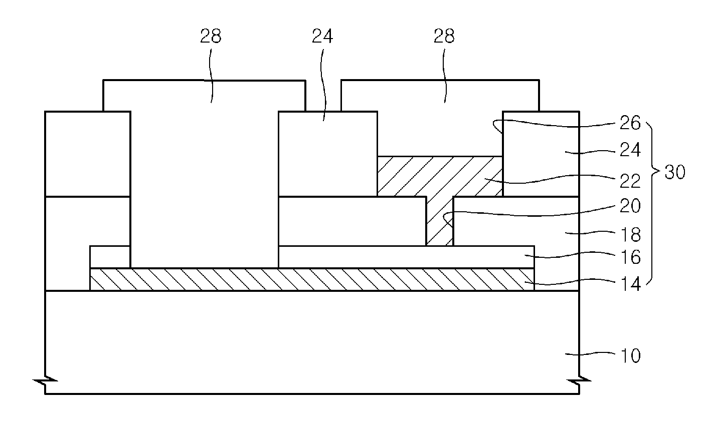
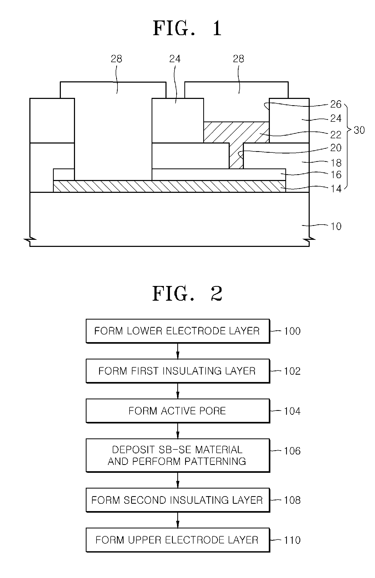
[0045]FIG. 1 is a sectional view illustrating the structure of a phase-change memory device according to an embodiment of the present invention...


PUM

PropertyMeasurementUnit
widthaaaaaaaaaa
melting pointaaaaaaaaaa

Abstract

Provided are a phase-change memory device using a phase-change material having a low melting point and a high crystallization speed, and a method of fabricating the same. The phase-change memory device includes an antimony (Sb)-selenium (Se) chalcogenide SbxSe100-x phase-change material layer contacting a heat-generating electrode layer exposed through a pore and filling the pore. Due to the use of SbxSe100-x in the phase-change material layer, a higher-speed, lower-power consumption phase-change memory device than a GST memory device can be manufactured.

Description

CROSS-REFERENCE TO RELATED PATENT APPLICATION[0001]This application claims the benefit of Korean Patent Application No. 10-2005-0083420, filed on Sep. 7, 2005, in the Korean Intellectual Property Office, the disclosure of which is incorporated herein in its entirety by reference.BACKGROUND OF THE INVENTION[0002]1. Field of the Invention[0003]The present invention relates to a phase change nonvolatile memory device and a method of fabricating the same, and more particularly, to a phase-change memory device using a chalcogenide metal alloy composed of antimony (Sb) and selenium (Se), and a method of fabricating the same.[0004]2. Description of the Related Art[0005]Semiconductor memory devices are generally classified as either volatile or non-volatile. A DRAM (dynamic random access memory) is a typical volatile memory device. The DRAM needs a periodic refresh process to retain data. When the integration density of a memory device is low, the power consumption of the refresh process is...

Claims


Application Information

Patent Timeline
Patent Type & Authority Patents(United States)
IPC IPC(8): H01L29/08
CPCH01L45/06H01L45/1233H01L45/126H01L45/1683H01L45/1625H01L45/1675H01L45/143H10N70/231H10N70/8413H10N70/8825H10N70/826H10N70/026H10N70/066H10N70/063
Inventor YOON, SUNG MINLEE, NAM YEALRYU, SANG OUKLEE, SEUNG YUNPARK, YOUNG SAMCHOI, KYU JEONGYU, BYOUNG GON
Owner ELECTRONICS & TELECOMM RES INST
Why Eureka
Try Eureka