Eureka AIR delivers breakthrough ideas for toughest innovation challenges, trusted by R&D personnel around the world.

CMOS transceiver with dual current path VCO

Active Publication Date: 2009-06-23
LATTICE SEMICON CORP
View PDF11 Cites 14 Cited by
  • Summary
  • Abstract
  • Description
  • Claims
  • Application Information

AI Technical Summary

Benefits of technology

[0011]A quad-channel design of the present invention exhibits power, performance, and cost advantages and offers a small footprint in many high bandwidth communication systems such as Gigabit Ethernet, Fibre Channel, network switch, etc. While sharing a single phase-locked loop (PLL) among multiple channels requires chip-wide clock distribution and potentially causes clock-waveform distortion, a local PLL dedicated to each channel alleviates clock-distribution problem. However, inter-channel noise coupling must be minimized with a careful power / ground design in both die and BGA-package levels.
[0012]In the quad design of a preferred embodiment with 8 independent PLLs, compared with a 2.5-V design, the tuning range of a voltage-controlled oscillator (VCO) is sufficiently wider, thereby guaranteeing correct operation in extremely varying process, voltage, and temperature (PVT) conditions. Furthermore, unlike a conventional VCO with a similar supply voltage (1.8 V) and tuning range, which has too large a VCO gain (Kv), this low jitter transceiver incorporates a Kv reduction technique and thus exhibits low jitter performance.

Problems solved by technology

While sharing a single phase-locked loop (PLL) among multiple channels requires chip-wide clock distribution and potentially causes clock-waveform distortion, a local PLL dedicated to each channel alleviates clock-distribution problem.
Furthermore, unlike a conventional VCO with a similar supply voltage (1.8 V) and tuning range, which has too large a VCO gain (Kv), this low jitter transceiver incorporates a Kv reduction technique and thus exhibits low jitter performance.

Method used


Image

  • CMOS transceiver with dual current path VCO
  • CMOS transceiver with dual current path VCO
  • CMOS transceiver with dual current path VCO

Examples


Embodiment Construction

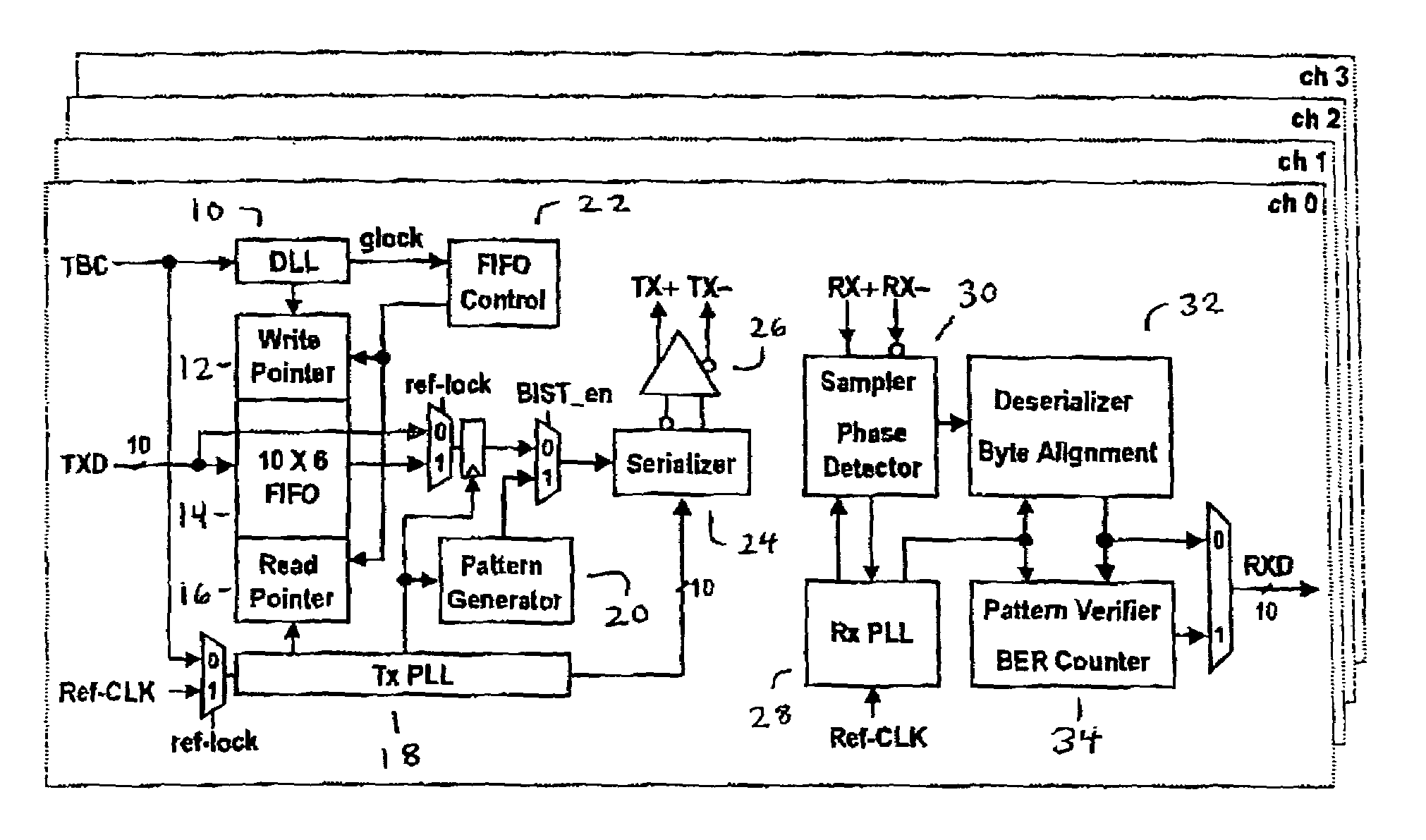
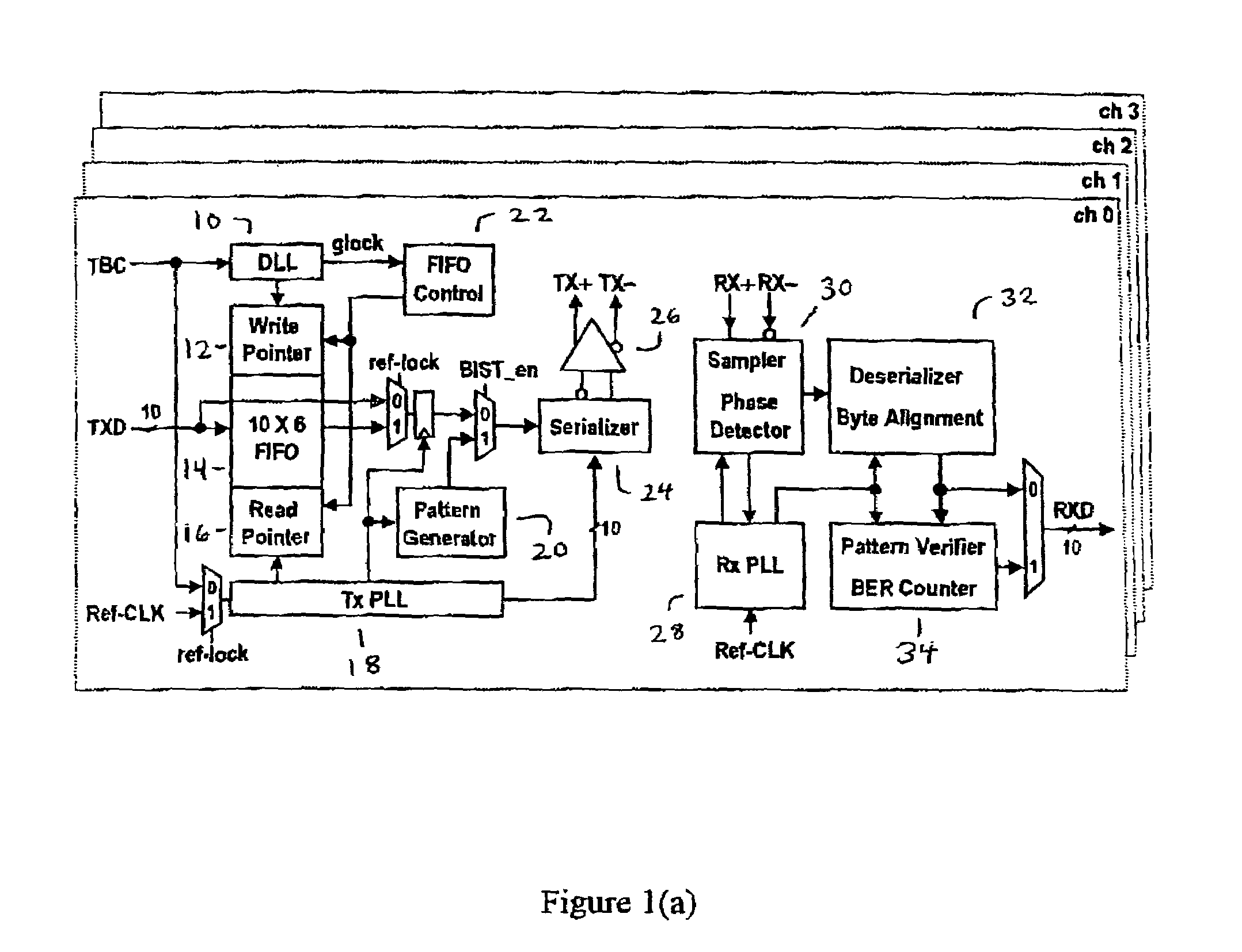
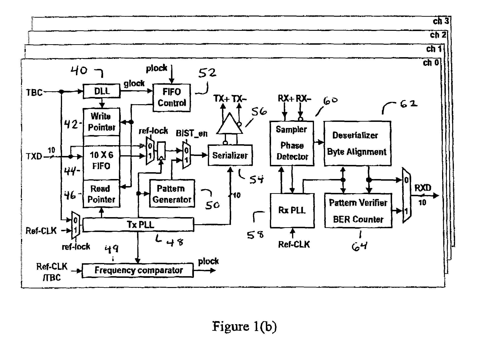
[0031]FIG. 1(a) shows a block diagram of one channel of the quad transceiver A delay locked loop (DLL) 10, is operatively connected to a write pointer 12, a 10×6 FIFO buffer 14, a read pointer 16, and a FIFO controller 22 on the transmitter side of the transceiver. Also shown are a transmitter phase locked loop (TxPLL) 18, a pattern generator 20, a serializer 24, and an output amplifier 26. In this embodiment the TxPLL 18 provides multiphase clocks to a serializer 24 and an additional clock to the other digital circuits. Since the transmit byte clock (TBC) and transmit data signals (TXD) have a predetermined phase relationship, if TBC is selected as the TxPLL input, the TXD signal can bypass a first-in / first-out (FIFO) circuit, thereby reducing the latency. However, since the TBC is provided by an ASIC protocol-device, it has a potentially larger jitter than a reference clock Ref-CLK. The receive portion contains a sampler phase detector 30, a receive phase locked loop (RxPLL) 28, a...


PUM


Abstract

A dual current path voltage controlled oscillator exhibits both the seamless frequency acquisition and uniform VCO gain reduction while preserving an original operating range and phase locked loop characteristics. The present invention provides a quad-channel transceiver comprising a phase locked loop circuit including a voltage controlled oscillator used to generate a clock signal, a FIFO buffer used to store data to be transmitted, a frequency comparator for comparing a reference clock to the generated clock signal from the phase locked loop circuit; and a folded starved inverter circuit contained within the voltage controlled oscillator wherein the folded starved inverter provides two current paths. The dual current paths allow for simultaneous coarse and fine phase tracking. With this low jitter performance and wide operating range, the quad transceiver may be implemented in 0.18-μm CMOS technology, and shows 10−12 bit error rate up to speeds of 3 Gbps.

Description

CROSS REFERENCE TO RELATED APPLICATIONS[0001]This application is related to and claims benefit from co-pending provisional application “A CMOS Transciever with Dual Current Path VCO” Ser. No. 60 / 406,858 filed Aug. 29, 2002, the complete contents of which are herein incorporated by reference.BACKGROUND OF THE INVENTION[0002]This invention relates generally to integrated circuits, and more particular to integrated circuits utilizing CMOS transceiver technology.[0003]Tranceivers (transmitters / receivers) are used in integrated circuits to communicate with circuitry off and / or on the integrated circuit chips. However, transceivers of the prior art tend to be rather complex, which increases the “footprint” on the integrated circuit chip. Prior art transceivers also have power, performance and cost issues.[0004]Considerable research effort has focused on implementing the physical layers of Gigabit Ethernet, Fibre Channel, IEEE 1394, network switch, etc. The major goal is to give the physic...

Claims


Application Information

Patent Timeline
IPC IPC(8): H04B1/06
CPCH03L7/087H03L7/0891H03L7/0995H03L7/0818H03L7/1072H03L7/0816
Inventor MOON, YONGSAMPARK, YOUNG SOOJEONG, DEOG-KYOON
Owner LATTICE SEMICON CORP
Why Eureka
Eureka Blog
Learn More