Interposing structure

a technology of interposer and integrated circuit, which is applied in the direction of electrical apparatus contruction details, semiconductor/solid-state device details, printed circuit non-printed electric components association, etc., can solve the problems of insufficient measures, inconvenient installation, and insufficient resistance of long power supply lines, and achieves a thick structure

Inactive Publication Date: 2009-07-28
XILINX INC
View PDF66 Cites 65 Cited by
  • Summary
  • Abstract
  • Description
  • Claims
  • Application Information

AI Technical Summary

Benefits of technology

[0020]In one aspect, vias of a via caposer extend through the caposer from a top surface of the caposer to a bottom surface of the caposer. There is one such via that extends from each of the micro-bumps on the die and down to a corresponding one of a set of landing pads on the package. Because signal conduction through the caposer is provided by these vias, metal from the micro-bumps on the die does not have to extend from the surface of the die above, all the way through through-holes in the caposer, and to the landing pads below. This signal path is instead provided by a via. Accordingly, a via caposer can be made thicker than a through-hole caposer. Because a via caposer can be a relatively thick structure, the often expensive semiconductor processing technologies needed to make a thin caposer are not required. Rather, a via caposer can be made using relatively inexpensive printed circuit board fabrication processes and materials.

Problems solved by technology

At these higher frequencies, transient currents are significantly higher than in the past, and parasitic inductance is a much more important issue.
However, as operating frequencies continue to increase, even these measures become inadequate.
In addition to the issues set forth above, an active circuit disposed on an integrated circuit die typically draws spikes of current from local power supply lines on the integrated circuit die.
Where the active circuit is disposed in the center of the integrated circuit die, however, the long power supply line can have significant resistance and inductance.
Accordingly, the voltage on the VCC power lead of the active circuit drops momentarily when the active circuit draws a spike of current and results in undesirable consequences.
Due to the drop in the voltage on the VCC power lead, the active circuit may be momentarily unable to output a digital logic high voltage.
Unfortunately, power supply problems in certain applications of an integrated circuit are often not properly anticipated during the design stage of the integrated circuit.
Refabricating an integrated circuit is generally a very expensive process.
Adding bypass capacitance by redesigning and laying out the integrated circuit can be exceedingly expensive and slow.
In addition to the problem of having to provide bypass capacitance for an already-designed integrated circuit, there also sometimes exists a problem where the interconnections between the terminals on the integrated circuit and signal traces on the printed circuit are to be changed.
The printed circuit board may be designed incorrectly such that traces on the printed circuit board are coupled to the wrong integrated circuit package terminals.
In addition to the bypass capacitance and signal redistribution problems set forth above, problems with impedance mismatch sometimes exist.
For example, where the output impedance of a driving circuit on an integrated circuit differs significantly from a characteristic impedance of a signal line onto which the driving circuit drives a signal, undesirable reflections may be generated.
Similar undesirable reflections may also be generated where the input impedance of a receiving circuit on the integrated circuit differs significantly from a characteristic impedance of a signal line through which the signal is supplied to the receiving circuit.
Because a via caposer can be a relatively thick structure, the often expensive semiconductor processing technologies needed to make a thin caposer are not required.

Method used


Image

  • Interposing structure
  • Interposing structure
  • Interposing structure

Examples


Embodiment Construction

[0056]In the following description, numerous specific details are set forth to provide a more thorough understanding of the present invention. However, it will be apparent to one skilled in the art that the present invention can be practiced without these specific details.

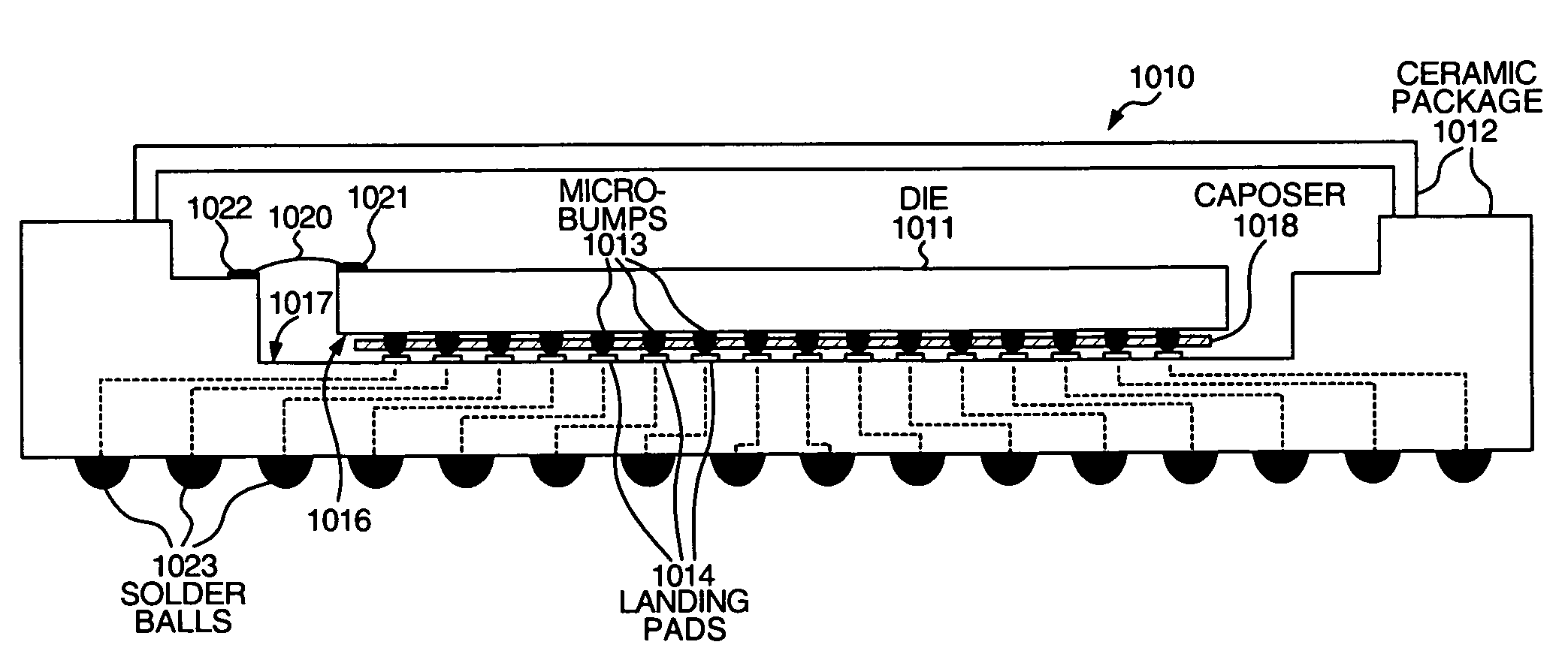
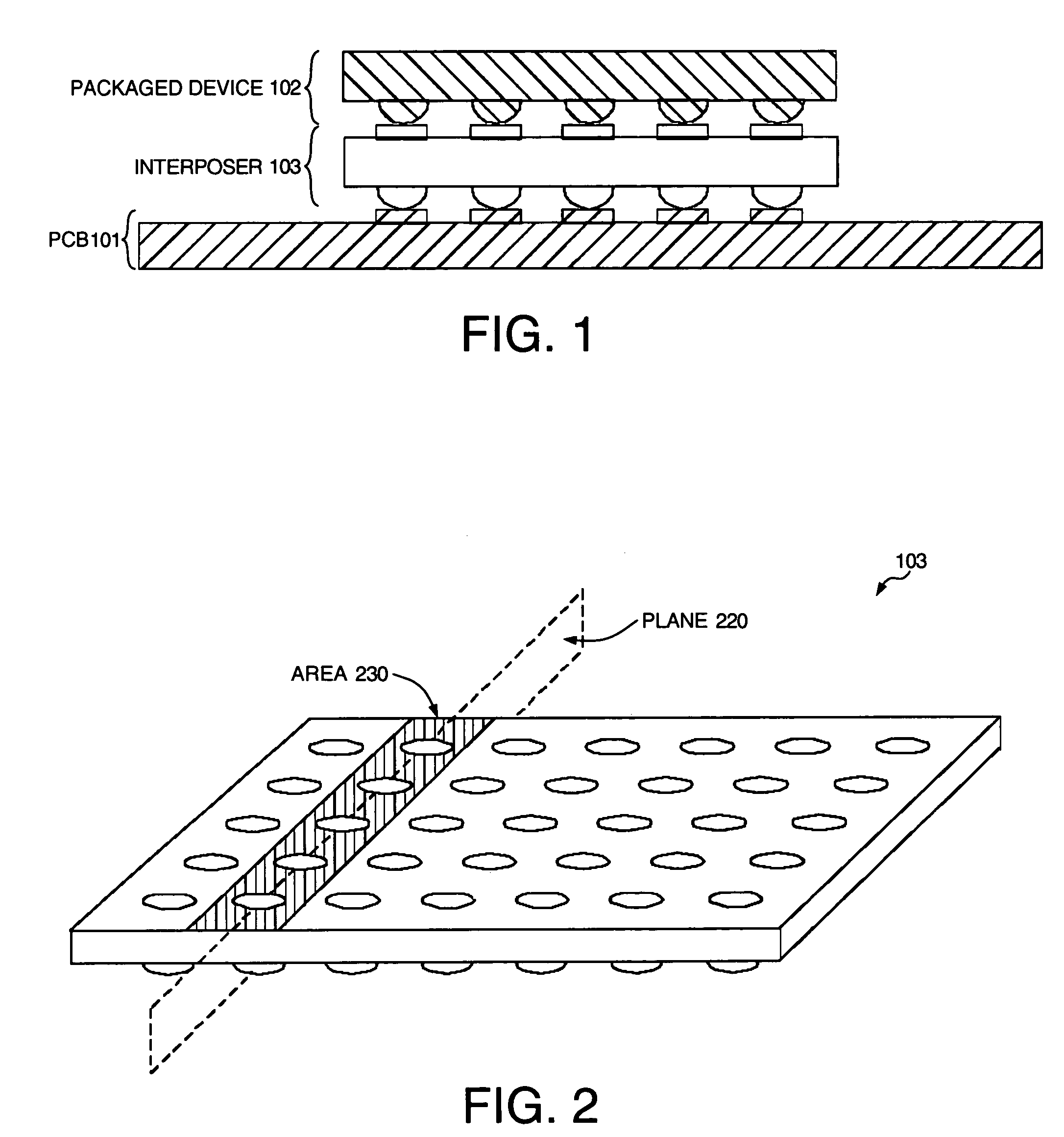
[0057]FIG. 1 is a cross-sectional side view of a packaged integrated circuit (IC) 102 mounted on a printed circuit board (PCB) 101 using a capacitive interposer 103 according to one embodiment of the invention. In the pictured embodiment, packaged IC 102 comprises a ball grid array (BGA) package. Interposer 103 is a multi-layered parallel-plate capacitive device having an array of lands on one side and a corresponding array of balls on the other. The balls on the bottom surface of interposer 103 are mounted (e.g., soldered) to lands on PCB 101 using commonly known techniques. Similarly, the balls of packaged IC 102 are mounted (e.g., soldered) to the lands on the top surface of interposer 103.

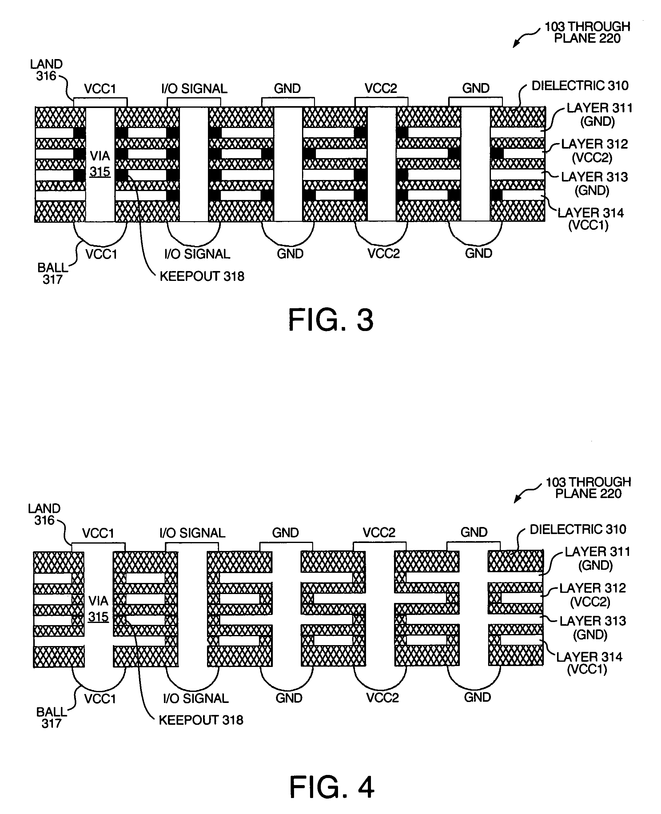
[0058]The lands and ba...


PUM


Abstract

A capacitive interposer (caposer) is disposed inside an integrated circuit package between a die and an inside surface of the package. Conductive layers within the caposer constitute a bypass capacitor. In a through-hole caposer, micro-bumps on the die pass through through-holes in the caposer and contact corresponding landing pads on the package. As they pass through the caposer, power and ground micro-bumps make contact with the plates of the bypass capacitor. In a via caposer, power and ground micro-bumps on the die are coupled to power and ground landing pads on the package as well as to the plates of the bypass capacitor by power and ground vias that extend through the caposer. In signal redistribution caposer, conductors within the caposer redistribute signals between die micro-bumps and package landing pads. In an impedance matching caposer, termination structures within the caposer provide impedance matching to a printed circuit board trace.

Description

FIELD OF THE INVENTION[0001]The present invention relates to an interposer disposed inside an integrated circuit package between a die and the package, wherein the interposer provides bypass capacitance, signal redistribution functionality and / or signal termination structures close to the semiconductor die.BACKGROUND INFORMATION[0002]Systems that include integrated circuit (IC) devices typically include decoupling capacitors (also known as bypass capacitors) as well. A typical decoupling capacitor is a capacitor coupled between the power and ground pins (i.e., terminals) of a packaged IC to reduce noise on the power system within the IC. While in some cases the IC itself includes some decoupling capacitance, the amount of capacitance required is such that one or more additional discrete decoupling capacitors are usually added external to the packaged device.[0003]In the past, the location of these discrete decoupling capacitors was a less important issue. The switching frequency of ...

Claims


Application Information

Patent Timeline
Patent Type & Authority Patents(United States)
IPC IPC(8): H05K1/02H01L23/02H05K1/00
CPCH01L23/055H01L23/49827H01L23/642H01L24/16H01L24/81H01L2224/16227H01L2224/16235H01L2224/1624H01L2224/73257H01L2224/81191H01L2224/81192H01L2924/01013H01L2924/01029H01L2924/01078H01L2924/01082H01L2924/09701H01L2924/14H01L2924/1433H01L2924/15153H01L2924/15165H01L2924/1517H01L2924/15174H01L2924/15311H01L2924/15787H01L2924/16152H01L2924/19041H01L2924/19043H01L2924/30105H01L2924/30107H01L2924/3011H01L2924/01006H01L2924/01019H01L2924/01033H01L2924/01075H01L2924/014H01L23/49822H01L23/50Y10S257/924H01L2224/16265H01L2924/19103H01L2924/12036H01L2924/00
Inventor CONN, ROBERT O.
Owner XILINX INC
Why Eureka
Try Eureka