Aerosol deposition process

Active Publication Date: 2009-08-25
FUJITSU LTD +1
View PDF32 Cites 13 Cited by
  • Summary
  • Abstract
  • Description
  • Claims
  • Application Information

AI Technical Summary

Benefits of technology

[0022]Accordingly, it is a general object of the present invention to provide a novel and useful

Problems solved by technology
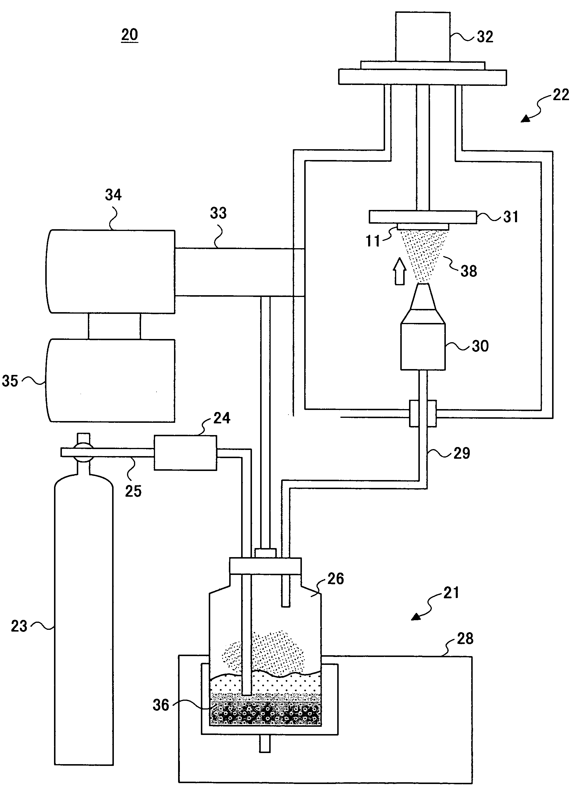
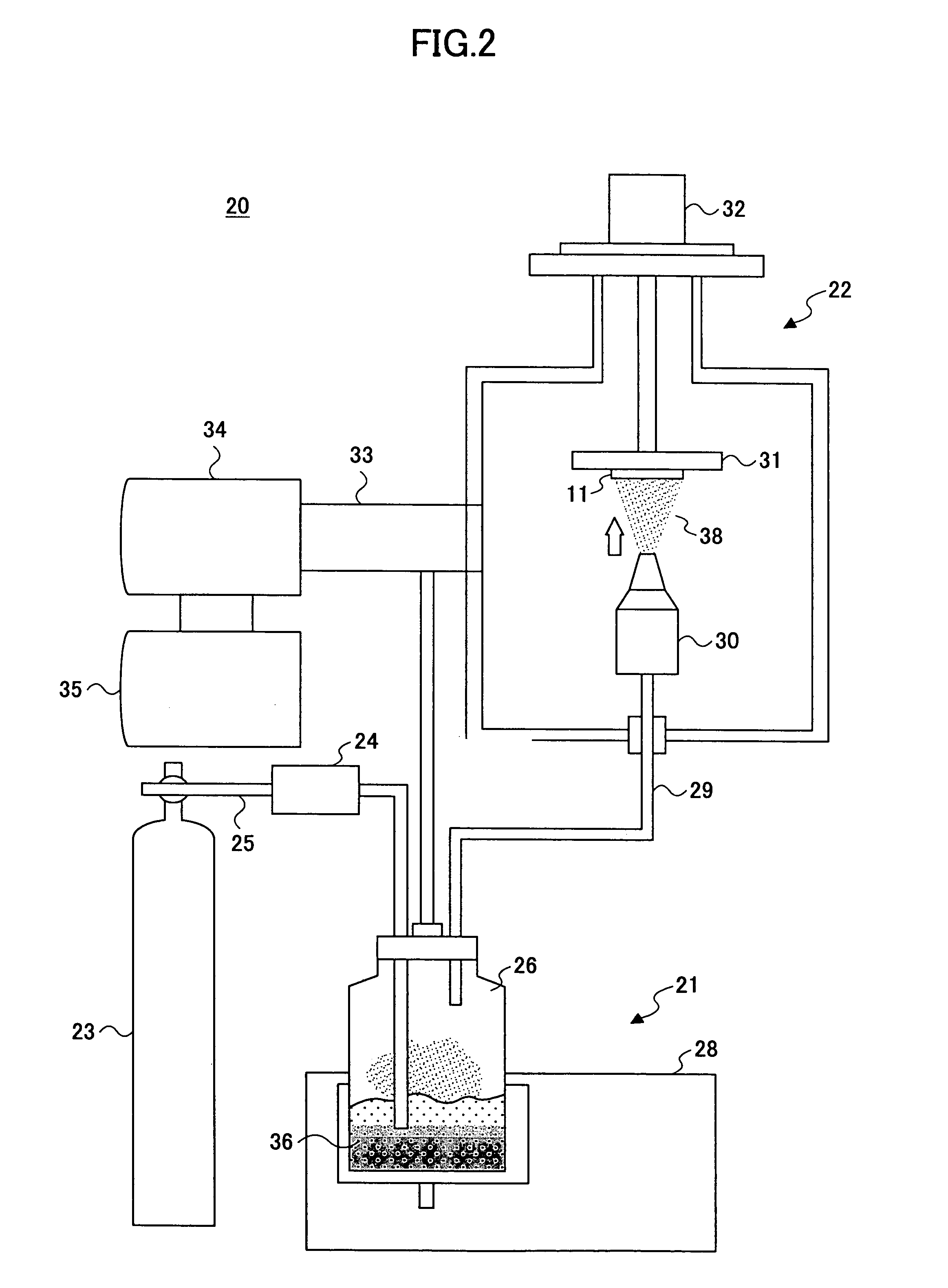
In the case of using polyimide as the insulation layer, on the other hand, it is necessary to reduce the temperature of the substrate heating down to 350° C. or lower for securing the reliability of the circuit substrate in view of the fact that the heat resistant temperature of polyimide is only about 400° C. However, in the case that the substrate heating process or post annealing process is conducted below the temperature of 350° C., crystallization of the dielectric film does not proceed sufficiently and there arises a problem in that the dielectric characteristics of the dielectric film is substantially inferior as compared to the case of a bulk material.
Thereby, there arises a problem in that the electrostatic capacitance of the capacitor is reduced.
However, such an approach can form only one layer of the dielectric film, and there arises a problem in that the electrostatic capacitance formed in the circuit substrate is limited.
With regard to the circuit substrate that forms the passive elements by using a ceramic substrates according to the type (2), there arise the problem of high cost due to the need of using high temperature over 1000° C. at the time of the baking process.
Further, there arises the problem of poor yield caused by possible short circuit, electrical disconnection, deformation, and the like, which in turn may be caused at the time of the baking process as a result of large difference of thermal expansion coefficients between the insulation fil

Method used


Image

  • Aerosol deposition process
  • Aerosol deposition process
  • Aerosol deposition process

Examples


first embodiment

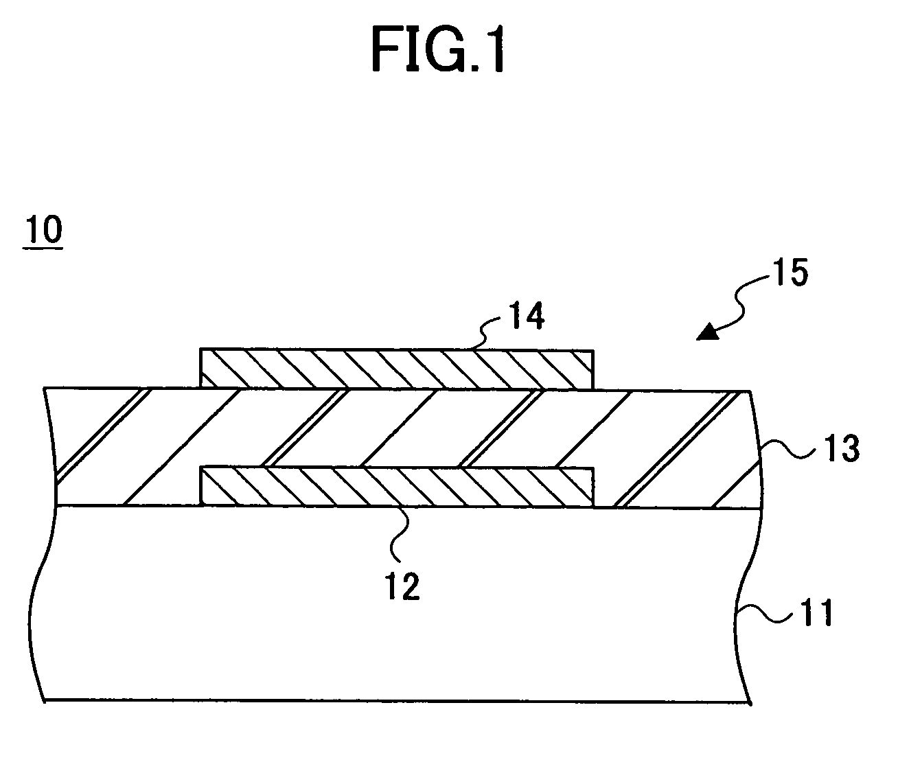
[0097]FIG. 1 is a cross-sectional diagram of a circuit substrate according to an embodiment of the present invention.

[0098]Referring to FIG. 1, the circuit substrate 10 of the present invention is formed of a base substrate 11, a first electrode layer 12 formed selectively on a surface of the base substrate 11, a dielectric film 13 covering the base substrate 11 and the first electrode layer 12, a second electrode layer 14 formed on the dielectric film 13 so as to oppose the first electrode layer, and thus, there is formed a capacitor 15 by the first electrode layer 12 and the second electrode layer 14 sandwiching the dielectric film 13.

[0099]For the base substrate 11, it is possible to use a resin material such as epoxy resin, polyimide, polyester resin, fluorine copolymer, a fiber glass, Teflon (trade mark), and the like. Of course, it is possible to use a metallic material of an alloy containing Fe, Ni, Mo, W, Al, Cu, Ag, Au, and the like, for the base substrate 11 by providing a...

second embodiment

[0123]FIG. 4 is a cross-sectional diagram showing a part of a circuit substrate 40 according to a second embodiment of the present invention.

[0124]Referring to FIG. 4, the circuit substrate 40 of the present invention is formed of an insulation layer 41, interconnection layers 42A and 42B formed selectively on the surface of the insulation layer 41, a resistance film 43 formed between the interconnection layers 42A and 42B, and the like, wherein the resistance body film 43 forms the resistance element 44.

[0125]Here, it should be noted that the resistance film 43 is formed by an AD process.

[0126]In the present embodiment, it is possible to form a resistance film of an oxide ceramic that does not require high temperature sintering process at the temperature of 1000° C. or more, by forming the resistance film by the AD process while using the fine particle material of ruthenium oxide (RuO2), and the like, which is generally used as a resistance material. Because the present invention d...

third embodiment

[0129]FIG. 5 is an exploded diagram showing a circuit substrate 44 according to a third embodiment of the present invention, while FIG. 6 is a cross-sectional diagram the circuit substrate 44.

[0130]Referring to FIGS. 5 and 6, the circuit substrate 44 of the present invention is formed of laminated insulation layers 45A-45D, a conductor film 46 formed on the insulation layer 45A, an inductor element 48 of a conductive material formed selectively on the insulation layer 45C with a the spiral pattern, and interconnection layers 47B and 47D connecting the conductor film 46 and the inductor element 48 or the inductor element 48 and other conductor films (not shown) electrically.

[0131]Similarly to the first and second embodiments, the insulation layers 45A-45D are formed of an organic or inorganic insulation layer such as epoxy resin insulation layer, polyimide insulation layer, and the like.

[0132]The inductor element 48 is formed of a conductive material of Cu having a thickness of 200 n...


PUM


Abstract

A circuit substrate includes a passive element and an interconnection pattern, wherein any of the passive element and the interconnection pattern is formed by an aerosol deposition process that uses aerosol of a fine particle material.

Description

CROSS-REFERENCE TO RELATED APPLICATION[0001]The present application is based on Japanese priority applications No.2003-137398 filed on May 15, 2003, No.2003-137399 filed on May 15, 2003 and No.2003-170475 filed on Jun. 16, 2003, the entire contents of which are hereby incorporated by reference.BACKGROUND OF THE INVENTION[0002]The present invention relates to circuit substrates having a passive element such as a capacitance element, a resistance element, an inductance element, and the like, thereon or therein, or an electron device having such a circuit substrate, or a fabrication process of such a circuit substrate. More particularly, the present invention relates to a circuit substrate having a base substrate or insulation layer formed of a resin material. Further, the present invention relates to circuit substrates, passive components, electron devices and the fabrication process of a circuit substrate suitable for use in a high frequency circuit. Particularly, the present inventi...

Claims


Application Information

Patent Timeline
IPC IPC(8): H01L21/8222H01L21/48H01L23/498H01L27/08H05K1/16H05K3/46
CPCH01L21/4857H01L23/49822H01L23/49894H01L27/08H05K1/162H01L21/4867H01L2224/16235H01L2224/16H01L2924/01004H01L2924/0102H01L2924/01046H01L2924/01077H01L2924/01078H01L2924/01079H01L2924/04941H01L2924/09701H01L2924/12044H01L2924/15192H01L2924/15311H05K1/167H05K3/4602H05K2201/0179H05K2201/0209H05K2201/09672H05K2203/1366H01L2924/01087H01L2924/19041H01L2924/19105H01L2924/00014H01L2224/0401
Inventor IMANAKA, YOSHIHIKOAKEDO, JUNLEBEDEV, MAXIM
Owner FUJITSU LTD
Why Eureka
Try Eureka