

Apparatus and method for electroforming high aspect ratio micro-parts
a micro-part and electroforming technology, applied in the field of apparatus and equipment for holding and positioning workpiece molds, can solve the problems of inability to easily or reliably use a device, poor electrical connection of one or more contacts with the wafer plating surface, and non-uniformity of the deposited electrically conductive layer, etc., to achieve quick and easy electrical contact
- Summary
- Abstract
- Description
- Claims
- Application Information
AI Technical Summary
Benefits of technology
Problems solved by technology
Method used
Image

Examples
example
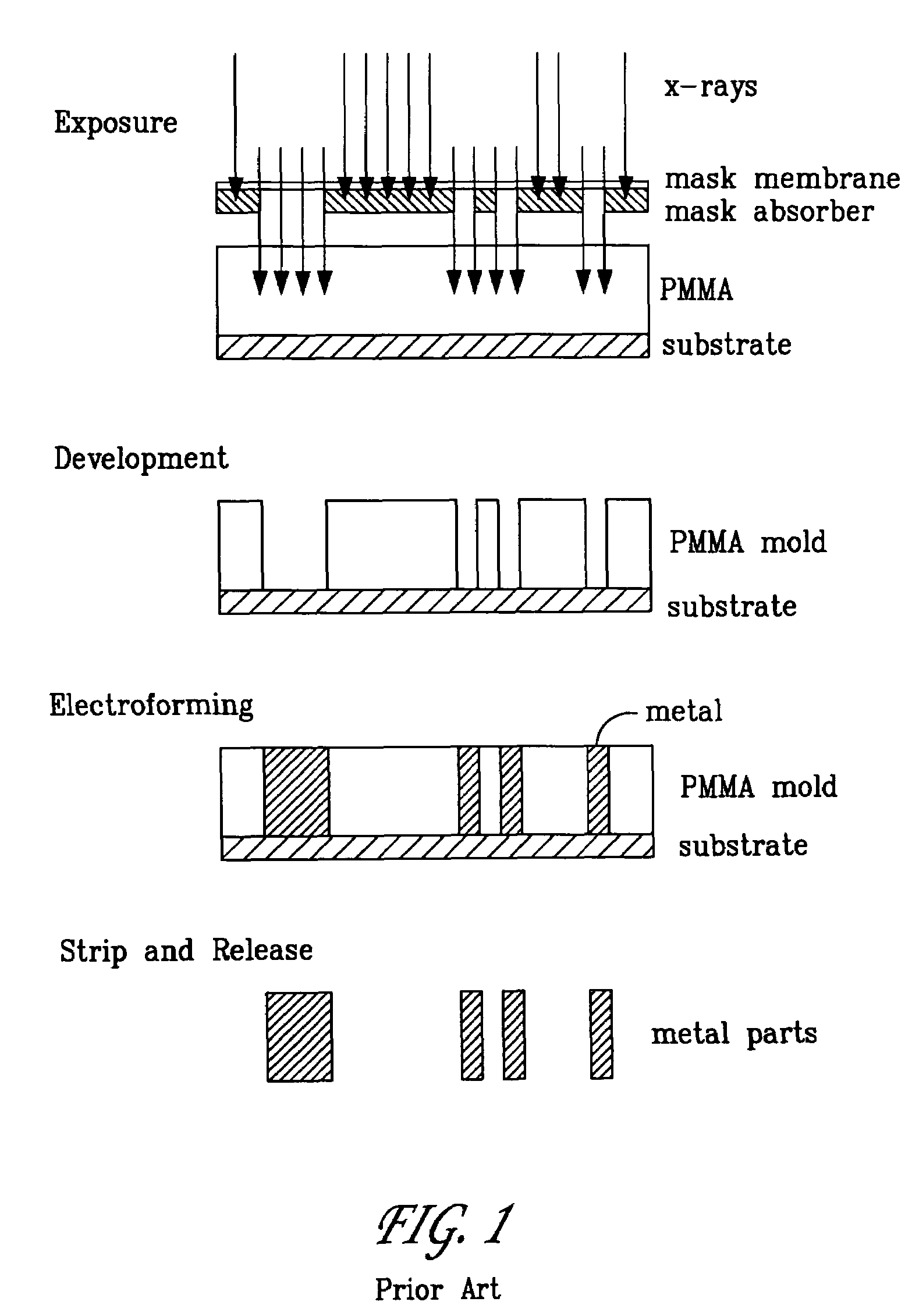
Ni / Mn Spring
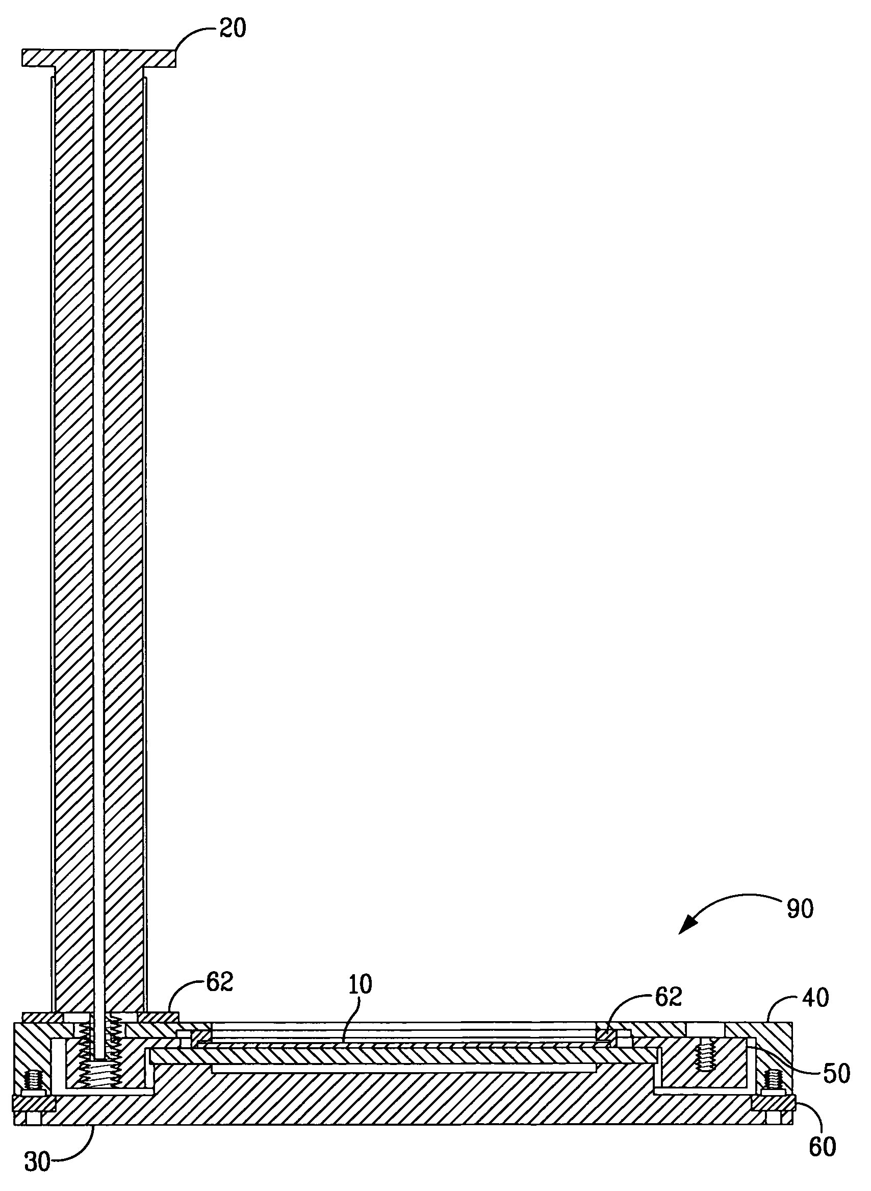
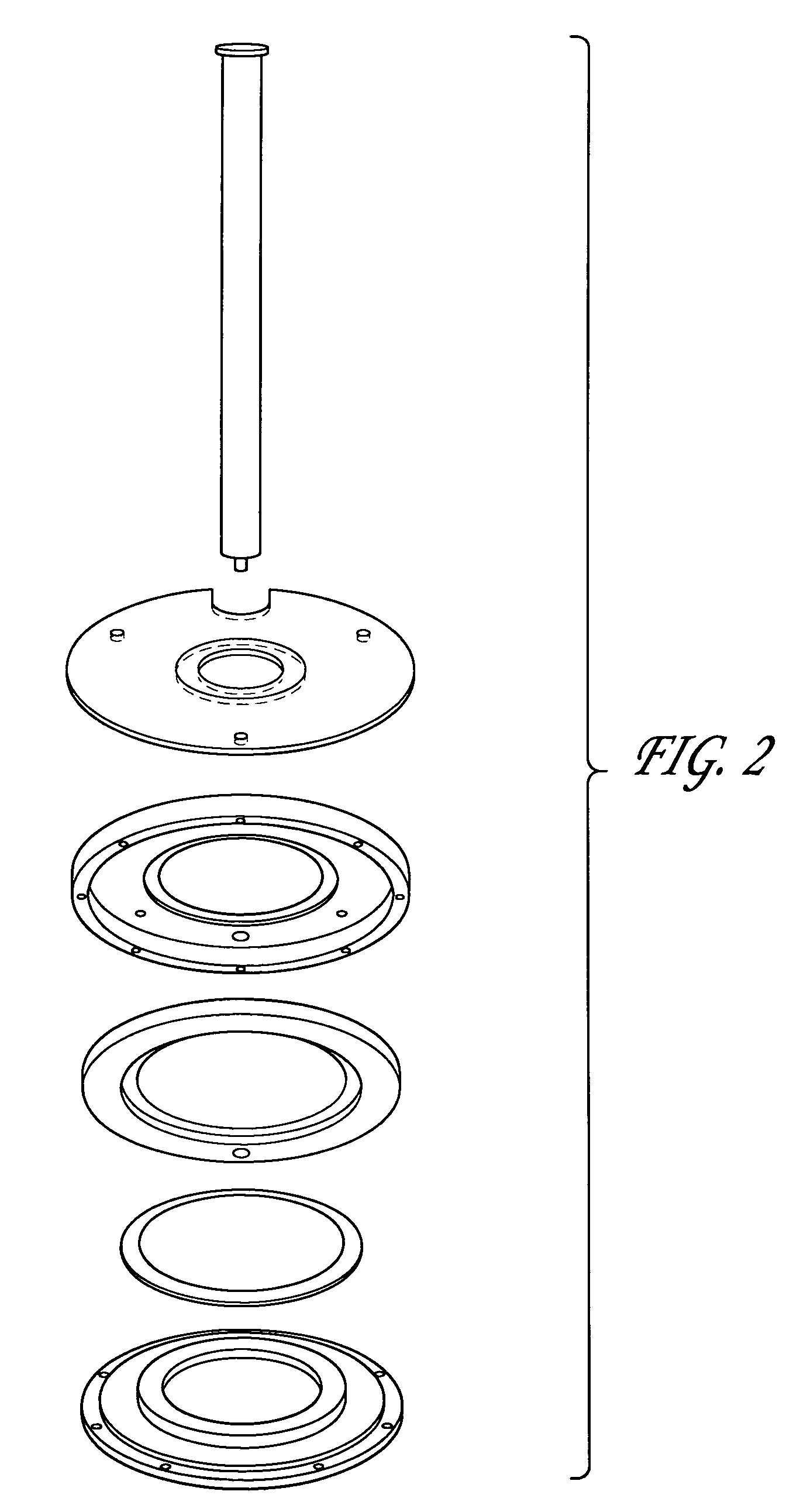
[0055]In order to demonstrate the utility of the present embodiment a mold was prepared for providing a number of miniature nickel-manganese springs. A 100 mm silicon wafer was coated with a metal conductive layer comprising a 70 nm thick titanium layer on a 400 nm thick copper layer and another 70 nm titanium layer over the copper layer as described in commonly-owned U.S. Pat. No. 6,517,665, herein incorporated by reference. The outer titanium layer is then chemically stripped and a 1 mm thick×82 mm diameter piece PMMA mold 5 is bonded onto substrate 3 over the conductive layer using a PMMA-based glue developed at Forschungszentrum Karlsruhe (FZK). The adhesive consisted of 10 g of 15% by weight PMMA (950 kg / mol) in MMA, 0.1 g N,N-dimethyl aniline, 0.1 g 3-(trimethoxysilyl)propyl methacrylate (MEMO), and 0.1 g benzoyl peroxide. This was degassed under a vacuum of 22 mmHg for a few minutes before application, and the bond interface was loaded to 450 kPa (65 psi) with a p...
PUM
| Property | Measurement | Unit |
|---|---|---|
| Electrical conductor | aaaaa | aaaaa |
| Metallic bond | aaaaa | aaaaa |
| Electric field | aaaaa | aaaaa |
Abstract
Description
Claims
Application Information