Vapor deposition of metal carbide films

a metal carbide film and vapor deposition technology, applied in the field of metal carbide thin film vapor deposition, can solve the problems of insufficient thin film coverage in shaded areas of complex substrate contours, high relative temperature of substrates, and difficult to obtain important film coverage in deep vias, etc., and achieve the effect of plasma-enhanced atomic layer deposition process

Active Publication Date: 2009-11-03
ASM IP HLDG BV
View PDF164 Cites 450 Cited by
  • Summary
  • Abstract
  • Description
  • Claims
  • Application Information

AI Technical Summary

Problems solved by technology

This makes film coverage in deep vias important but difficult to obtain.
A problem with the disclosed process is that the substrate temperature is rather high relative to thermal budgets for state-of-the-art semiconductor fabrication, particularly in metallization stages.
Line-of-sight deposition, however, means that complex substrate contours will have insufficient thin film coverage in shaded areas.
Problems with prior art methods of forming metal carbide films include difficulties in forming films with low impurity contents.
Depending on the precursor used, metal carbon films may include high halogen, oxygen and / or carbon impurities, which significantly reduce film quality and device performance.
Although ALD is capable of forming uniform metal carbide films on geometrically challenging structures, producing high quality (i.e. low impurity) films may be difficult to achieve with prior art methods.

Method used


Image

  • Vapor deposition of metal carbide films
  • Vapor deposition of metal carbide films
  • Vapor deposition of metal carbide films

Examples


example

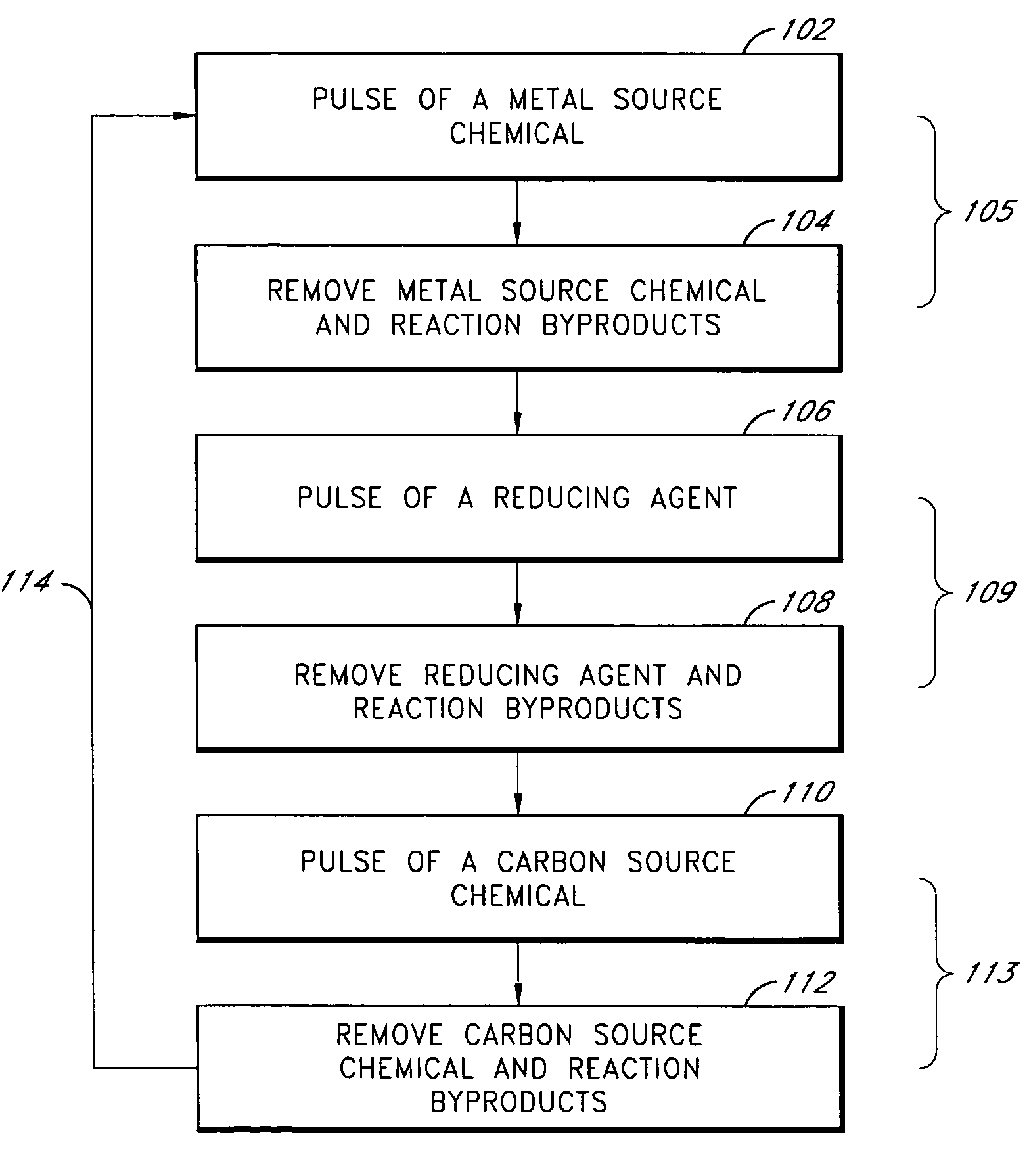
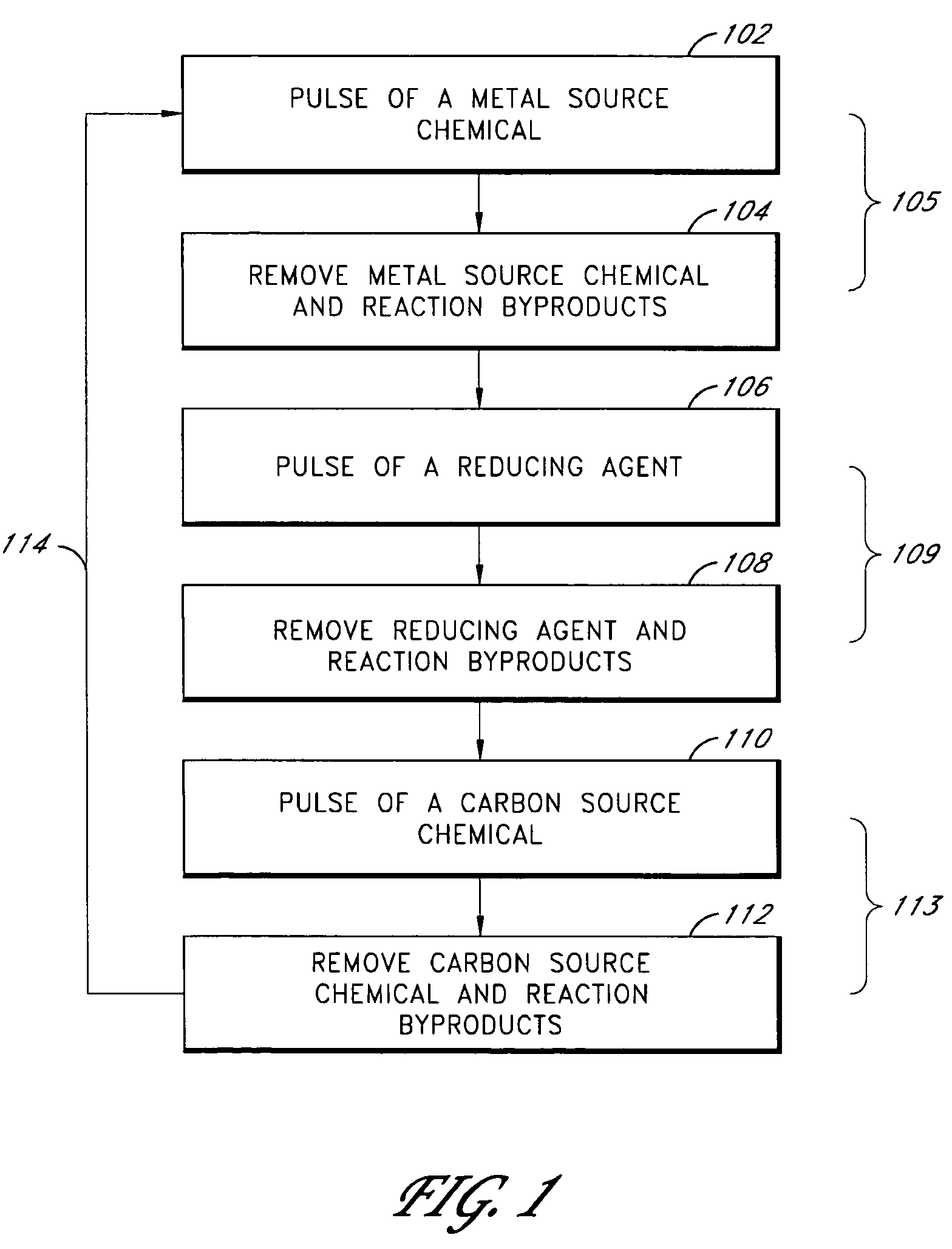
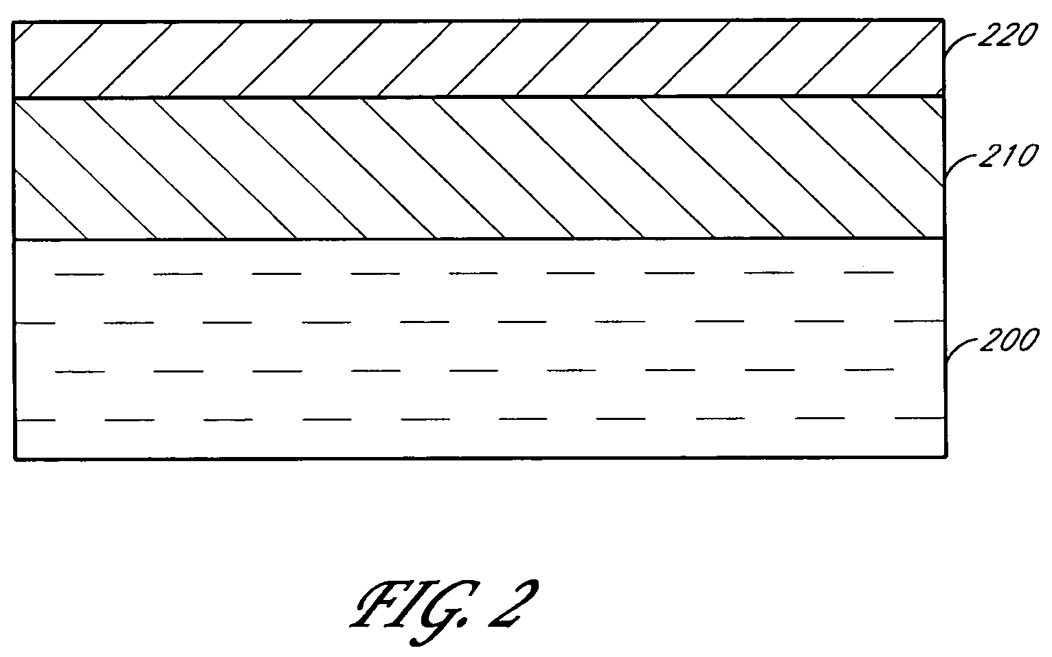
[0069]A tantalum carbide film was deposited on a silicon dioxide (SiO2) substrate in an ALD-type process. The sequence of steps included alternately and sequentially contacting a silicon substrate comprising native oxide with spatially and temporally separated vapor phase pulses of tantalum fluoride (TaF5), hydrogen radicals (“H2*”) and a carbon source chemical (TEB or C2H2). The substrate was supported on a susceptor in a PEALD reactor. Deposition was conducted at a susceptor temperature between about 300° C.-350° C. The reactor pressure was about 3 torr. The TaF5 source gas was held at a temperature of about 125° C. Argon (Ar) was introduced into the reactor at a flow rate of approximately 650 sccm and served as a carrier and purge gas. H2* was generated by supplying plasma power (about 100-400 W) to a showerhead disposed over the substrate while flowing hydrogen gas. The showerhead temperature was maintained at about 250° C. The sequence of gas pulses and pulsing times (milliseco...


PUM

PropertyMeasurementUnit
thicknessaaaaaaaaaa
thicknessaaaaaaaaaa
thicknessaaaaaaaaaa

Abstract

Methods of forming metal carbide thin films are provided. According to preferred embodiments, metal carbide thin films are formed in an atomic layer deposition (ALD) process by alternately and sequentially contacting a substrate in a reaction space with spatially and temporally separated vapor phase pulses of a metal source chemical, a reducing agent and a carbon source chemical. The reducing agent is preferably selected from the group consisting of excited species of hydrogen and silicon-containing compounds.

Description

BACKGROUND OF THE INVENTION[0001]1. Field of the Invention[0002]The present invention relates generally to the field of semiconductor manufacturing and, in particular, to forming metal carbide thin films using atomic layer deposition (ALD).[0003]2. Description of the Related Art[0004]The integration level of components in integrated circuits is increasing, producing a need for smaller components, including interconnects. Design rules are dictating a feature size less than or equal to 0.2. μm. This makes film coverage in deep vias important but difficult to obtain.[0005]The trend of decreasing feature size is evident, for example, in memory circuits or devices such as dynamic random access memories (DRAMs), flash memory, static random access memories (SRAMs), ferroelectric (FE) memories, and integrated circuit components, such as gate electrodes and diffusion barriers in complementary metal oxide semiconductor (CMOS) devices.[0006]Metal carbides have found widespread use in the elect...

Claims


Application Information

Patent Timeline
Patent Type & Authority Patents(United States)
IPC IPC(8): C23C16/00
CPCC23C16/32C23C16/45542C23C16/45534C23C16/45527
Inventor ELERS, KAI-ERIK
Owner ASM IP HLDG BV
Why Eureka
Try Eureka