Thin-film transistor and manufacturing method thereof

a thin film transistor and manufacturing method technology, applied in the field of thin film transistors, can solve the problems of large leakage current, decrease in throughput, and inability to use amorphous silicon thin film to form tfts, and achieve the effects of low leakage current amount, high contrast ratio of lcd, and high quality

Active Publication Date: 2009-11-17
NEC LCD TECH CORP
View PDF11 Cites 2 Cited by
  • Summary
  • Abstract
  • Description
  • Claims
  • Application Information

AI Technical Summary

Benefits of technology

[0055]The second embodiment provides the same advantageous effects as those of the first embodiment described above. In addition, according to the second embodiment, an LDD-TFT with minimum leakage current can be fabricated with fewer processes than the first embodiment because a gate electrode consisting of a lower layer having a relatively wide profile and an upper layer having a relatively narrow profile can be formed in a single photoresist process.
[0056]While LDD region 19 is provided on both of the source and drain sides of the channel region formed beneath the gate electrode in the first and second embodiments, the LDD region may be provided only on the drain side according to the present invention. In that case, only a source-drain region with a relatively high impurity concentration will be formed on the source side in the polysilicon thin film.
[0057]According to the present invention, while the gate electrode in the embodiments described above has a two-layer structure consisting of lower gate electrode 14 made from a microcrystalline silicon thin film and upper gate electrode 15 made from a metal film, a gate electrode consisting of a lower layer having a wider profile and an upper layer having a narrower profile may be formed by processing a single-layer film made from the same material. Furthermore, the lower gate electrode itself may be formed with a multilayer film, and the upper gate electrode itself may be formed with a multilayer film. The order in which the upper and lower gate electrodes are formed is not limited to the order described above. The lower gate electrode may be patterned first and then the upper gate electrode may be patterned.
[0058]FIG. 6 shows an exemplary configuration of an LCD including LDD-TFTs according to the present invention. LCD 30 shown includes insulating substrate 31 on which TFTs according to the first or second embodiment are formed, counter substrate 32 paired with insulating substrate 31, display portion 33 including multiple liquid-crystal elements (not shown) sandwiched between insulating substrate 31 and counter substrate 32, and circuits such as driving circuits (such as scan circuit 34) for driving the liquid-crystal elements through the TFTs. The circuits provided include scan circuits 34, 37, level shifter / timing buffer 35, level shifter 36, data register 38, latch circuit 39, DAC (digital-to-analog converting) circuit 40, selector circuit 41 and the like. Details of a configuration of the driving circuits used are well-known to those skilled in the art and are disclosed, for example, in Japanese Patent Laid-Open Application No. 2004-46054 (JP, A, 2004-046054).
[0059]Display portion 33 includes a matrix of gate lines 42 and data lines 43, TFTs each of which provided at an intersection of gate line 42 and data line 43, and liquid-crystal elements connected to the TFTs. Display portion 33 is configured as an active-matrix display. The TFTs constituting the circuits such as driving circuits are polysilicon LDD-TFTs formed on insulating substrate 31 at the same time as the formation of other TFTs (i.e., pixel transistors) each of which is associated with each individual liquid-crystal pixel in display portion 33.
[0060]LCD 30 is low-cost and yet capable of displaying a high-quality image because it has display portion 33 formed with LDD-TFTs according to any of the embodiments described above. This is because the TFTs according to the present invention can achieve low leakage current amounts and therefore allow a high contrast ratio of the LCD to be set and can reduce color nonuniformity, thus providing a high-quality picture even though they are manufactured with fewer processes. Furthermore, by using LDD-TFTs according to the present invention in driving circuits, malfunctions of the circuits can be prevented and the power consumption in the circuits can be reduced because leakage current is minimized.EXAMPLES

Problems solved by technology

It is undesirable to use an amorphous silicon thin film to form TFTs for driving circuits in terms of the operating speed and driving ability of the transistors.
However, one of the serious problems with polysilicon TFTs is a large leakage current.
However, the conventional LDD-TFTs have a problem that their manufacturing process sequence involves increased numbers of processes and masks required, resulting in a decrease in the throughput.
However, the overlapped LDD-TFTs have a problem that leakage current reduction, which is the intended purpose of the LDD, cannot sufficiently be achieved because a current leaks from the portion where the gate electrode and the LDD region overlap each other.
Although the overlapped LDD-TFT described in JP, A, 11-307777 can be manufactured by a simple manufacturing process, an increase in leakage current from the overlapping portion that occurs when a reverse voltage is applied is too large to be neglected.
If leakage current occurs in TFTs used in an LCD, liquid-crystal elements in individual pixels cannot adequately be controlled.

Method used


Image

  • Thin-film transistor and manufacturing method thereof
  • Thin-film transistor and manufacturing method thereof
  • Thin-film transistor and manufacturing method thereof

Examples


example 1

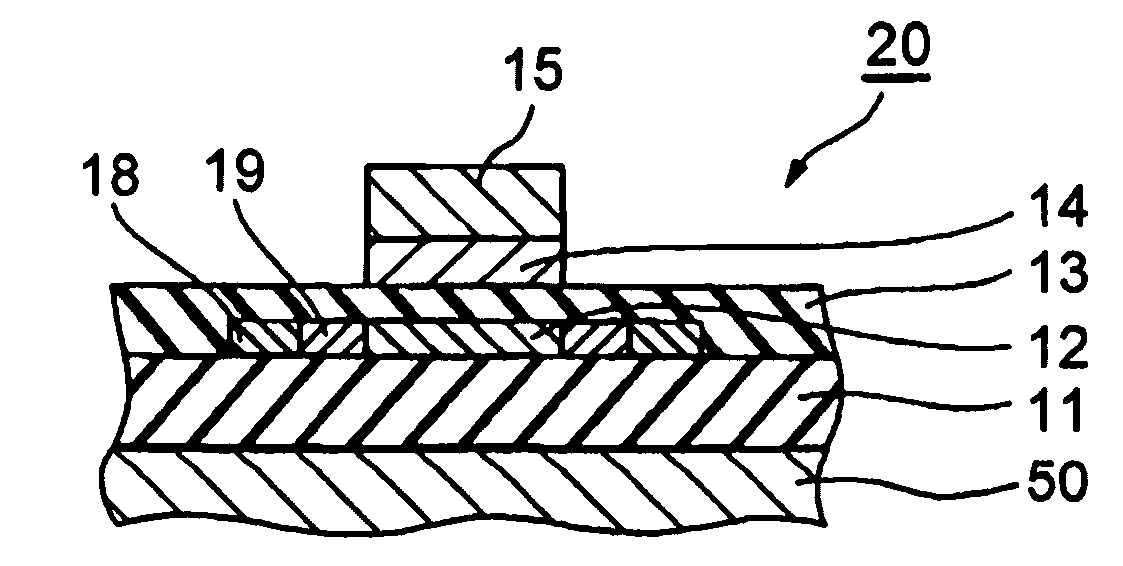
[0062]An LDD-TFT was manufactured according to the first embodiment. As insulating substrate 50 was used as a low-temperature glass, “OA-2 substrate” from Nippon Electric Glass Co., Ltd. A silicon dioxide thin film was deposited to a thickness of 300 nm on the low-temperature glass substrate as underlying insulating film 11 by using plasma CVD using a mixed gas of SiH.sub.4 and N.sub.2O as a raw-material gas. Then, an amorphous silicon thin film was deposited to a film thickness of 60 nm on underlying insulating film 11 by a reduced pressure CVD method using Si.sub.2H.sub.6 as a raw-material gas. The deposition was performed at a Si.sub.2H.sub.6 flow rate of 200 sccm under a pressure of 13 Pa at a substrate temperature of 450 degree C. for 50 minutes. After that, laser annealing was performed in which the amorphous silicon thin film was irradiated with a XeCl excimer laser beam with a wavelength of 308 nm to crystallize the amorphous silicon thin film, thereby forming a polysilicon ...

example 2

[0075]An LDD-TFT was manufactured according to the second embodiment.

[0076]As in Example 1, polysilicon thin film 12 was formed on a low-temperature glass substrate and was patterned into an island, and gate insulating film 13, microcrystalline silicon thin film 14A, and chromium thin film 15A were deposited. Then, a gate electrode was patterned as in Example 1. However, upper gate electrode 15 was overetched by using wet etching. The etchant used was an aqueous solution of diammonium cerium (IV) nitrate (Ce(NH4)2(NO3)6) and perchloric acid at room temperature and the etching was performed for 210 seconds. Photoresist film 16 used in the previous process was left and used to dry-etch lower gate electrode 14 under the same conditions used in Example 1. As a result, upper gate electrode 15 became narrower in width than lower gate electrode 14 by 1 μm on each side.

[0077]In this example, the amount of side-etching of the upper gate electrode was able to be increased by wet etching compa...


PUM


Abstract

A method for forming a thin-film transistor on an insulating substrate includes the steps of: forming a non-single-crystal semiconductor thin film on the insulating substrate; forming a gate insulating film on the non-single-crystal semiconductor thin film; forming a gate electrode including a lower gate electrode and an upper gate electrode on the gate insulating film, the lower gate electrode having a portion that is not covered by the upper gate electrode; forming a source-drain region and an LDD (lightly doped drain) region in the non-single-crystal thin film semiconductor film concurrently by introducing an impurity into the non-single-crystal semiconductor thin film through the gate electrode and the gate insulating film; and etching away an exposed portion of the lower gate electrode by using the upper gate electrode as a mask.

Description

BACKGROUND OF THE INVENTION[0001]1. Field of the Invention[0002]The present invention relates to a thin-film transistor (TFT) formed on an insulating substrate and a manufacturing method thereof and, in particular, to a thin-film transistor suitable for use in a liquid-crystal display (LCD) and a contact image sensor and to a manufacturing method thereof.[0003]2. Description of the Related Arts[0004]An active-matrix substrate in which an amorphous silicon TFT is provided for each pixel as a pixel transistor has been used in most LCDs in recent years. However, as the variety of applications of LCDs has increased, there is a strong demand for thinner and smaller LCDs. To meet the demand, it is becoming popular to form driving circuits with TFTs on an active-matrix substrate. It is undesirable to use an amorphous silicon thin film to form TFTs for driving circuits in terms of the operating speed and driving ability of the transistors. Therefore, there is also a demand for formation of ...

Claims


Application Information

Patent Timeline
Patent Type & Authority Patents(United States)
IPC IPC(8): H01L21/20
CPCH01L29/42384H01L29/4908H01L29/78648H01L29/78621H01L29/6675
Inventor SATOU, TADASHI
Owner NEC LCD TECH CORP
Why Eureka
Try Eureka