
Method for forming underlying insulation film

a technology of underlying insulation film and film, which is applied in the direction of electrical equipment, semiconductor devices, capacitors, etc., can solve the problems of increasing leakage current, increasing power consumption, and unable to obtain good interfacial properties, so as to achieve easy control of film forming rate and film forming time. , the effect of easy control of the thickness of the underlying film

Inactive Publication Date: 2009-11-24
TOKYO ELECTRON LTD
View PDF15 Cites 2 Cited by
  • Summary
  • Abstract
  • Description
  • Claims
  • Application Information

AI Technical Summary

Benefits of technology

[0009]Another object of the present invention is to provide a process capable of forming a good underlying film at the interface between an insulating film and an electronic device substrate so as to improve the resultant transistor characteristic.
[0010]As a result of earnest study, the present inventors have found that, when an insulating film (for example, high-k material film) is once formed on an electronic device substrate and plasma based on a process gas comprising at least an oxygen atom-containing gas is caused to pass through the insulating film so as to form an underlying film at the insulating film-substrate interface, such a process is extremely effective in achieving the above-mentioned object, unlike the conventional technique wherein an underlying film is formed on an electronic device substrate and then an insulating film (for example, high-k material film) is formed thereon.
[0014]In the process for forming an underlying film according to the present invention having such a constitution, active plasma species (for example, oxygen reactive species) are caused to pass through the insulating film from the insulating film surface side to reach the insulating film-substrate interface, to thereby form an underlying film in the vicinity of the interface. In the present invention, the film-forming rate can be controlled (that is, the film-forming time can be controlled) easily, as compared with the case wherein an underlying film is directly formed on an electronic device substrate. Accordingly, in the present invention, it is easy to control the thickness of the underlying film and / or to improve the in-plane uniformity of the underlying film.

Problems solved by technology

This is because the leakage current of a certain degree can cause a severe problem in the recent devices which have attained finer structures, and / or higher performances, even when the leakage current of such a degree have actually caused substantially no problem in the conventional devices having a lower degree of integration.
Particularly, in view of the development in the mobile or portable-type electronic devices in a so-called “ubiquitous” society of recent construction (i.e., information-oriented society wherein people can use a network service, anytime and anywhere, by means of electronic devices), it is necessary to develop a low-power consumption device, and therefore the reduction in the leakage current is an extremely important issue.
Typically, in a case where the formation of a finer structure in a high-performance silicon LSI is pursued, for example, for the purpose of developing a next-generation MOS-type transistor, there arises her performance a problem that the leakage current is increased and the resultant power consumption is also increased.
However, when such an insulating film, which has been expected to provide a good property, is actually formed by CVD (chemical vapor deposition method) or the like, particularly in the case of the formation of an insulating film having a very high practical utility (for example, a relatively thin insulating film of about 12 A (angstrom)), a good interfacial property can be hardly obtained between the insulating film and the underlying electronic device substrate.
However, it is very difficult to form such a thin underlying film directly on an electronic device substrate by using a conventional thermal oxidation or plasma oxidation technique (the thickness of a thin film can be hardly controlled by such a technique), while controlling the film-forming rate or in-plane uniformity.

Method used


Image

  • Method for forming underlying insulation film
  • Method for forming underlying insulation film
  • Method for forming underlying insulation film

Examples


embodiment of

One Embodiment of Production Process

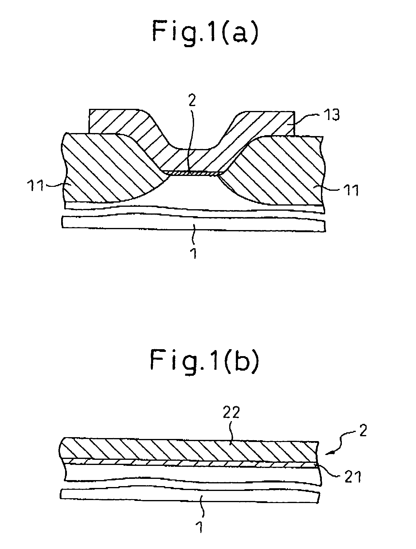
[0071]Next, the process for producing such an electronic device material comprises a gate insulator 2 and a gate electrode 13 is described below.

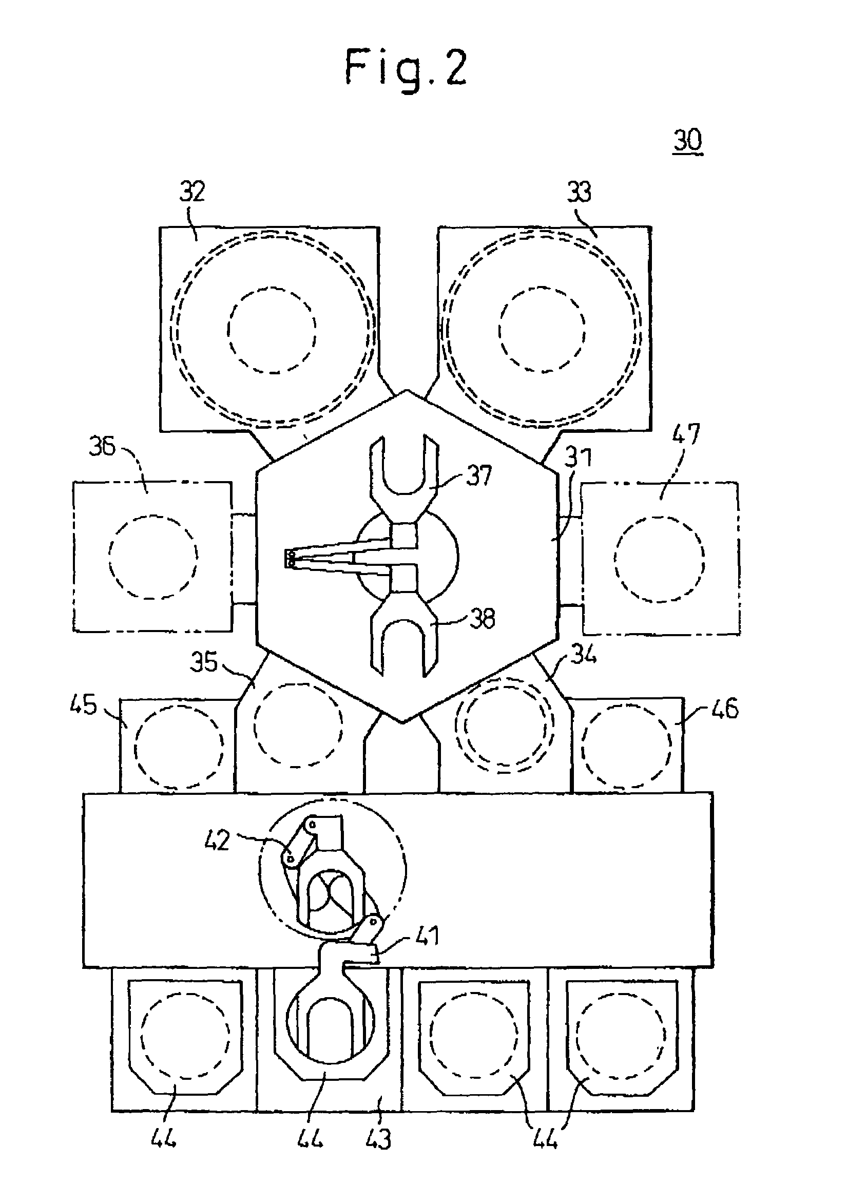
[0072]FIG. 2 is schematic view (schematic plan view) showing an example of the total arrangement of a semiconductor manufacturing equipment 30 for conducting the process for producing an electronic device material according to the present invention.

[0073]As shown in FIG. 2, in a substantially central portion of the semiconductor manufacturing equipment 30, there is disposed a transportation chamber 31 for transporting a wafer W (FIG. 2). Around the transportation chamber 31, there are disposed: plasma processing units 32 and 33 for conducting various treatments on the wafer, two load lock units 34 and 35 for conducting the communication / cutoff between the respective processing chambers, a heating unit 36 for operating various heating treatments, and a heating reaction furnace 47 for conducting various hea...

example 1

[0120]FIG. 14 and FIG. 15 show a change in the electrical film thickness (Teq) and in the uniformity of the electrical film thickness (range: difference between the maximum and minimum values of in-plane Teq), respectively, with respect to the oxidation time, when an oxidizing plasma processing is applied onto the HfSiO film and the oxide film formed by an RLSA oxidation process. Samples as shown in FIGS. 14 and 15 were produced by the following process.

(1) Substrate

[0121]A p-type silicon substrate having a resistivity of 8 to 12 Ωcm and a plane direction of (100) was used as the substrate. On the surface of the silicon substrate, a 500 A-sacrificial oxide film was formed by a thermal oxidization process.

(2) Pretreatment for HfSiO Film Formation

[0122]The sacrificial oxide film and contaminant factors (metals, organic materials and particles) were removed by RCA washing using a combination of APM (a mixed solution of ammonia, aqueous hydrogen peroxide and pure water), HPM (a mixed so...

example 2

[0127]The Cv property of the MOS capacitor which had been produced in Example 1 was evaluated. This measurement was performed by the following process. The CV property was evaluated for a capacitor having a gate electrode area of 10,000 μm2. The CV property was determined by evaluating the capacitance at each voltage in the process of sweeping the gate voltage from 1 V to about −2 V at a frequency of 1 MHz. From the thus determined CV property, the electrical film thickness was calculated.

[0128]FIG. 14 shows an electrical film thickness (Teq) when an oxidizing plasma processing is applied onto the HfSiO film and the oxide film formed by an RLSA oxidation process. The abscissa indicates an oxidation treatment time and the ordinate indicates an electrical film thickness (Teq).

[0129]As shown in FIG. 14, the reference oxide film reaches a film thickness of 25 A when the oxidation time is 20seconds or more. As the treatment time is shorter, the reproducibility of the process becomes lowe...


PUM


Abstract

The surface of an insulating film disposed on an electronic device substrate is irradiated with plasma based on a process gas comprising at least an oxygen atom-containing gas, to thereby form an underlying film at the interface between the insulating film and the electronic device substrate. A good underlying film is provided at the interface between the insulating film and the electronic device substrate, so that the thus formed underlying film can improve the property of the insulating film.

Description

TECHNICAL FIELD[0001]The present invention relates to a process for forming an insulating film having a good interfacial property. More specifically, the present invention relates to a method of irradiating an insulating film with plasma based on a process gas comprising at least an oxygen atom-containing gas, to thereby improve the interfacial property between the insulating film and the substrate. The modification process according to the present invention is suitably usable, particularly for a so-called high-k (high-dielectric constant) material.BACKGROUND ART[0002]In general, the present invention is widely applicable to the production of materials for electronic device such as semiconductors or semiconductor devices, and liquid crystal devices. For the convenience of explanation, however, the background art relating to semiconductor devices as an example of the electronic devices, will be described here.[0003]Substrates for semiconductors or electronic device materials such as ...

Claims


Application Information

Patent Timeline
Patent Type & Authority Patents(United States)
IPC IPC(8): H01L21/31H01L21/02H01L21/28H01L21/316H01L29/51
CPCH01L21/28185H01L21/28202H01L21/31604H01L21/28194H01L29/518H01L21/31662H01L28/56H01L29/517H01L21/31645H01L21/02211H01L21/02164H01L21/02271H01L21/02148H01L21/0234H01L21/02362
Inventor SUGAWARA, TAKUYATADA, YOSHIHIDENAKAMURA, GENJIOZAKI, SHIGENORINAKANISHI, TOSHIOSASAKI, MASARUMATSUYAMA, SEIJIHASEBE, KAZUHIDENAKAJIMA, SHIGERUFUJIWARA, TOMONORI
Owner TOKYO ELECTRON LTD
Learn More