Nonlinear element, element substrate including the nonlinear element, and display device

a nonlinear element and substrate technology, applied in static indicating devices, instruments, thermoelectric devices, etc., can solve the problems of difficult to make the thicknesses of insulating thin films used for all nonlinear elements uniform, difficult to drive the nonlinear elements at low voltage, and difficult to make uniform thicknesses of insulating thin films used for all nonlinear elements. , to achieve the effect of eliminating time, preventing nonlinear element characteristics, and improving reliability

Inactive Publication Date: 2009-12-01
SEMICON ENERGY LAB CO LTD
View PDF16 Cites 20 Cited by
  • Summary
  • Abstract
  • Description
  • Claims
  • Application Information

AI Technical Summary

Benefits of technology

[0013]In addition, by using the composite material of the present invention, an ohmic contact can be made, making it possible to use various kinds of materials for an electrode.
[0014]In addition, since the nonlinear element used in the present invention is formed by using a composite material, in which a voltage-current characteristic in a case of applying forward bias voltage and a voltage-current characteristic in a case of applying reverse bias voltage exhibit nonlinear behavior respectively, flicker and the like caused by difference in transmittance when inverting voltage applied to a liquid crystal, can be prevented.
[0015]Moreover, since resistance of the nonlinear element used in the present invention is less affected by variations in thickness of a layer containing a composite material as compared to an insulating thin film which has been used in a conventional nonlinear element, variations in characteristics of the nonlinear element can be prevented, thereby improving reliability.
[0016]Further, for the nonlinear element of the present invention, it is possible to eliminate time, which has been required for manufacturing an insulating thin film with a uniform thickness in a conventional nonlinear element, and hence, productivity can be improved.
[0017]Furthermore, driving voltage can be reduced so that a long-life nonlinear element can be provided.

Problems solved by technology

However, in a conventional nonlinear element using an insulating thin film, since the insulating thin film has high resistivity, it has been difficult to drive the nonlinear element at low voltage.
In addition, since an insulating thin film used in a conventional nonlinear element has different resistance depending on its difference in thickness of the insulating thin film, there have been problems such as variations in characteristics of the nonlinear element, and it has been necessary to make the thickness of the insulating thin film uniform.
However, it is difficult to make thicknesses of insulating thin films used for all nonlinear elements uniform, and it takes a long time to make the thicknesses uniform.
Thus, there has been also a problem of reduction in productivity.

Method used


Image

  • Nonlinear element, element substrate including the nonlinear element, and display device
  • Nonlinear element, element substrate including the nonlinear element, and display device
  • Nonlinear element, element substrate including the nonlinear element, and display device

Examples


embodiment mode 1

[0035]One mode of a structure of a nonlinear element of the present invention will be described.

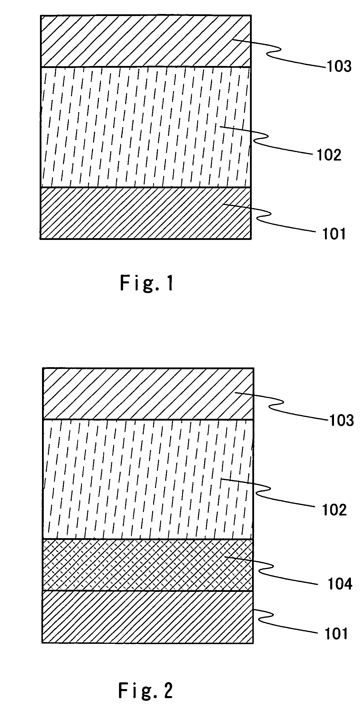
[0036]In this embodiment mode, an example of a structure of a nonlinear element of the present invention will be described with reference to FIG. 1. The nonlinear element of the present invention has a structure in which a layer 102 containing a composite material is provided between a first electrode 101 and a second electrode 103.

[0037]The first electrode 101 can be formed using various kinds of metal, alloys, electroconductive compounds, and mixed metal thereof. For example, indium tin oxide (ITO); indium tin oxide containing silicon oxide; or indium zinc oxide (IZO) in which 2 to 20 wt % zinc oxide (ZnO) is mixed in indium oxide; can be used. In addition, gold (Au); platinum (Pt); nickel (Ni); tungsten (W); chromium (Cr); molybdenum (Mo); iron (Fe); cobalt (Co); titanium (Ti); copper (Cu); palladium (Pd); aluminum (Al); aluminum-silicon (Al—Si); aluminum-titanium (Al—Ti); aluminum-sil...

embodiment mode 2

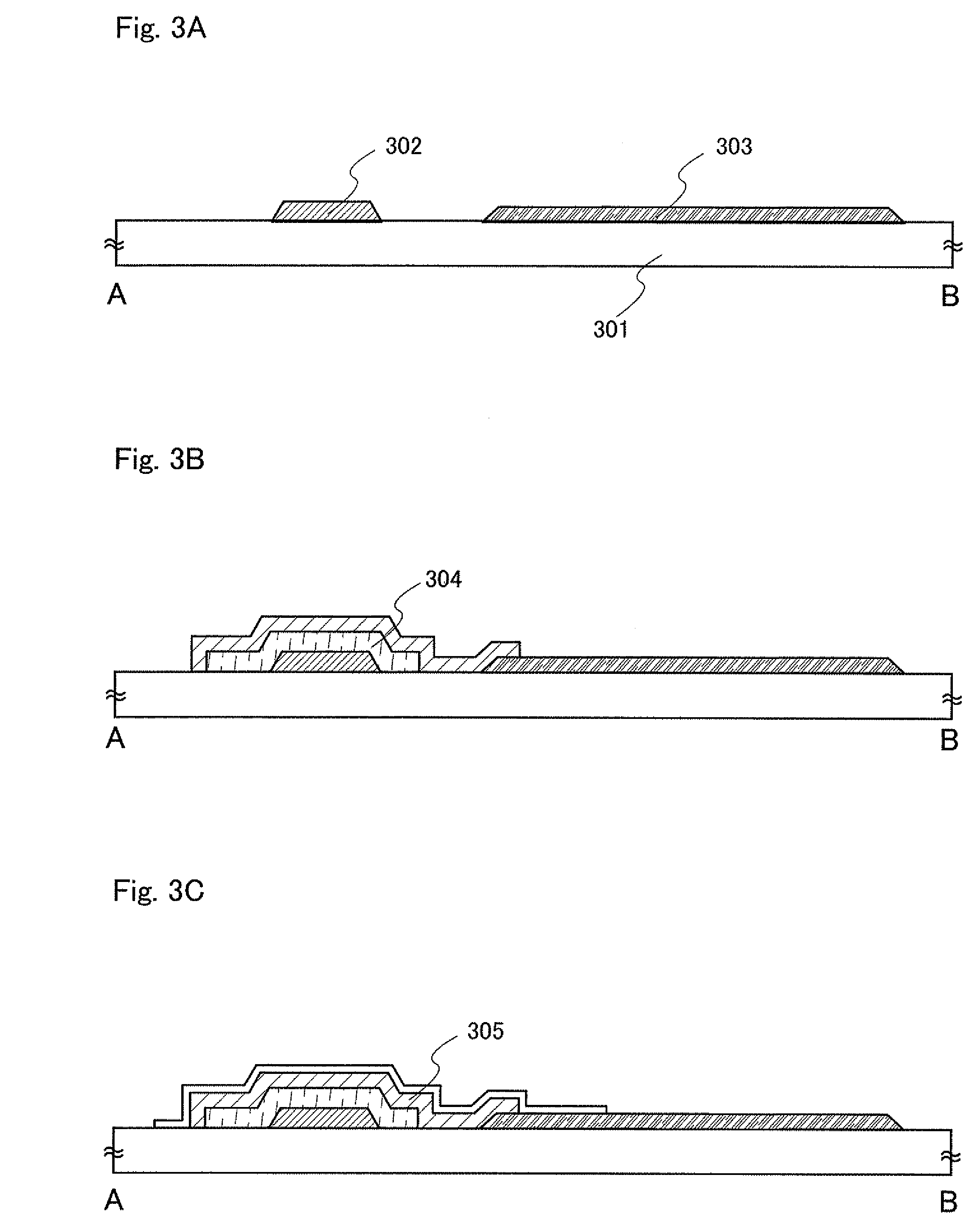
[0061]In Embodiment Mode 2, one mode of a structure of an element substrate including a nonlinear element of the present invention as described in Embodiment Mode 1, and a method for manufacturing thereof will be described. FIGS. 3A to 3C are cross sectional views along lines A-B of FIGS. 4A to 4C in respective steps, whereas FIGS. 4A to 4C are top views in the respective steps.

[0062]Over an insulating substrate 301, a first electrode 302 is formed to have a desired shape by using a technique for forming a pattern. The first electrode 302 may be formed using the materials mentioned in Embodiment Mode 1. Further, the method for forming the first electrode is not limited to the above method.

[0063]In this embodiment mode, an insulating substrate made from glass, plastic, quartz, or the like can be used. Further, a material of the element substrate including the nonlinear element of the present invention, is not limited to the above materials.

[0064]A predetermined pattern is formed over...

embodiment mode 3

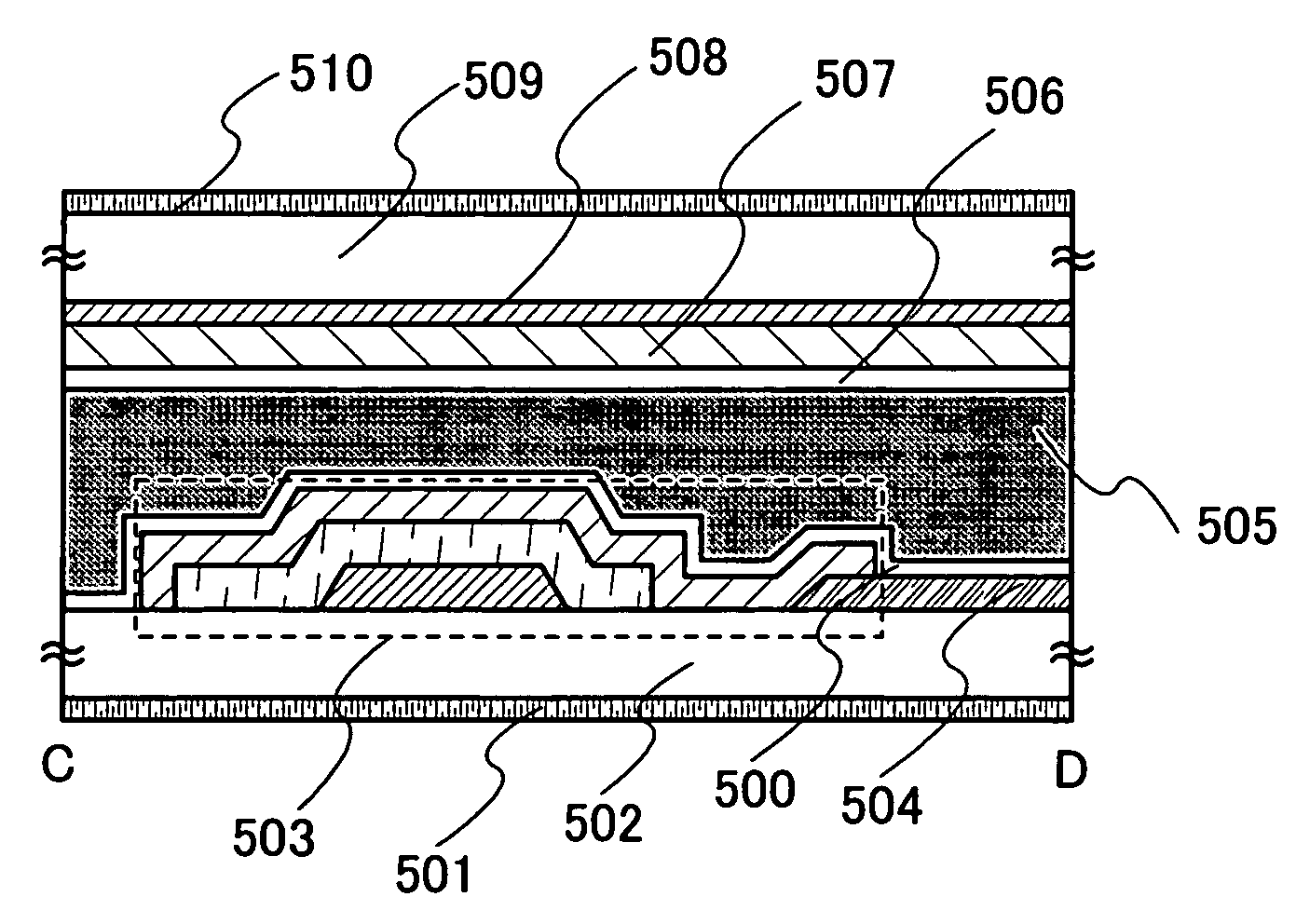
[0068]A liquid crystal display device can be manufactured by using a nonlinear element substrate of the present invention. In this embodiment mode, a method for manufacturing a liquid crystal display device will be described with reference to FIGS. 5A and 5B and FIGS. 6A to 6C. FIG. 5A is a top view showing a pixel region of a display device whereas FIG. 5B is a cross sectional view along a line C-D of FIG. 5A. FIG. 6A is also a top view of the display device and FIG. 6B is a cross sectional view along a line C-D of FIG. 6A. The same portions and portions having similar functions will not be explained repeatedly.

[0069]First, FIGS. 5A and 5B will be described. In the pixel region, a nonlinear element 503 of the present invention, and a pixel electrode 504 are provided over an insulating substrate 502 having a polarizing plate 501.

[0070]Next, an insulating layer 500, which is also referred to as an orientation film, is formed by printing or spin coating so as to cover a pixel electrod...


PUM

PropertyMeasurementUnit
distanceaaaaaaaaaa
distanceaaaaaaaaaa
temperatureaaaaaaaaaa

Abstract

The purpose of the present invention is to provide a nonlinear element with high productivity, which can be driven at low voltage, an element substrate including the nonlinear element, and a liquid crystal display device including the element substrate. A structure of the nonlinear element of the present invention includes a layer formed using a composite material containing an inorganic compound and an organic compound between a first electrode and a second electrode. Further, as the composite material containing the inorganic compound and the organic compound, a composite material, which exhibits nonlinear behavior in both cases of applying forward bias voltage and reverse bias voltage, is used.

Description

BACKGROUND OF THE INVENTION[0001]1. Field of the Invention[0002]The present invention relates to a nonlinear element, an element substrate including the nonlinear element, and a display device including the element substrate. In particular, the present invention relates to a liquid crystal display device using a nonlinear element as a switching element.[0003]2. Description of the Related Art[0004]In recent years, it has been considered to use nonlinear elements for liquid crystal display devices. An MIM (metal insulator metal) switching element, which includes a three-layered structure formed by stacking a lower conductive thin film, an insulating thin film, and an upper conductive thin film, is known as one of the nonlinear elements.[0005]As a conventional MIM switching element, a structure, as shown in FIG. 14, in which a lower conductive thin film 1002 is provided over a substrate 101 made from glass, an insulating thin film 1003 is provided over an entire surface, and an upper c...

Claims


Application Information

Patent Timeline
Patent Type & Authority Patents(United States)
IPC IPC(8): H01L51/10
CPCG02F1/1362H01L51/006H01L51/0054H01L45/00H10N70/00H10K85/622H10K85/633
Inventor HIRAKATA, YOSHIHARUSAKATA, JUNICHIROIKEDA, HISAOIWAKI, YUJIKAWAKAMI, TAKAHIRO
Owner SEMICON ENERGY LAB CO LTD
Why Eureka
Try Eureka