Multilayer printed wiring board and manufacturing method of the multilayer printed wiring board

a printing method and wiring board technology, applied in the direction of electrical apparatus construction details, electrical apparatus contruction details, etc., can solve the problems of difficult buffering of stress, difficult transmission of generated stress, and decrease in the degree of deterioration

Active Publication Date: 2009-12-01
IBIDEN CO LTD
View PDF18 Cites 38 Cited by
  • Summary
  • Abstract
  • Description
  • Claims
  • Application Information

AI Technical Summary

Benefits of technology

[0012]The multilayer printed wiring board including a portion in which a corrosion resistant layer is formed and a portion in which no corrosion resistant layer is formed mixedly in its conductive layer exposed on the front face thereof can obtain reliability more easily than a conventional multilayer printed wiring board in which the corrosion resistant layer is formed on all conductive portions exposed on the front face. When an IC chip is installed or under heat cycle condition or under high temperature at high humidity, its board is elongated / contracted due to an influence of temperature. Because the surface of the board is under the same condition in the conventional multilayer printed wiring board in which the corrosion resistant layer is formed on all conductive portions exposed on the front face, stress generated by elongation / contraction is transmitted easily. Thus, the stress is difficult to buffer. However, in the multilayer printed wiring board having solder pads in which the corrosion resistant layer is formed partially, the generated stress is difficult to transmit. As a consequence, the stress is easy to buffer. For the reason, the multilayer printed wiring board of the present invention can obtain reliability more easily for a long term as compared to the conventional printed wiring board.
[0072]Particularly, as evident from evaluation of electric connectivity and reliability upon drop test, the degree of deterioration can be reduced as compared to the conventional printed wiring board and as a consequence, reliability for a long term is easy to maintain thereby the reliability is unlikely to drop.

Problems solved by technology

Thus, the stress is difficult to buffer.
However, in the multilayer printed wiring board having solder pads in which the corrosion resistant layer is formed partially, the generated stress is difficult to transmit.
Because stress is buffered more as compared to the conventional printed wiring board in evaluating its electric connectivity and reliability upon drop test, the degree of deterioration decreases.
Because stiffness is obtained, fault of the printed wiring board like the warping of the board can be suppressed and when a component is mounted, contact failure or non-connection is difficult to generate between a conductive portion of the solder pad and an external terminal of any component.
Further, because an operation component such as a key pad makes contact with a land portion in which the corrosion resistant layer is formed, contact failure is difficult to occur despite repeated contacts.
Thus, any mounted component turn unlikely to receive the impact, so that faults such as drop of component become unlikely to occur.
A fault such as crack in the solder layer is more difficult to occur.
The reason is estimated to be that with elongation / contraction, the generated stress is buffered or the generated stress is more difficult to concentrate locally so that a fault such as crack is more difficult to occur.
Contact failure is difficult to be induced even if such an external terminal contacts repeatedly.
When an impact is received from outside due to the solder pad in which no corrosion resistant layer is formed is used at an electronic component mounting terminal, removal is difficult to occur between a conductive circuit exposed from the solder pad and an electronic component.
Particularly, because the impact is buffered by the solder layer for joining them as well, crack is unlikely to occur in the solder layer so that removal is difficult to occur.
Because connectivity of the component is obtained as a result, electric connectivity or functionality as a product is not lowered and the reliability is no lower than the conventional printed wiring board.
Further, because flatness of a bonding pad is held by the corrosion resistant layer, any fault is unlikely to occur at the time of bonding.
Thus, any mounted component becomes unlikely to receive the impact, so that a fault such as drop of component becomes unlikely to occur.
Further, connectivity with the external board and reliability about that are easy to obtain.
As a result, the reliability is hard to drop.
The reason is that if the thickness is less than 20 μm, its strength drops so that it is difficult to handle and at the same time, reliability to the electric insulation property drops, so that formation of the via hole may be difficult.
Conversely, if the thickness is over 600 μm, formation of a fine via hole or depending on a case, filling with conductive paste is difficult and at the same time, the board itself turns thick.
If the thickness of the copper foil is less than 5 μm, an end face of the via hole in the copper foil can be deformed when an opening for formation of the via hole is formed in the insulation base material by using a laser processing described later, so that a conductive circuit is difficult to form.
If the thickness of the copper foil is over 18 μm, a conductive circuit pattern of fine lines is difficult to form by etching.

Method used


Image

  • Multilayer printed wiring board and manufacturing method of the multilayer printed wiring board
  • Multilayer printed wiring board and manufacturing method of the multilayer printed wiring board
  • Multilayer printed wiring board and manufacturing method of the multilayer printed wiring board

Examples


first embodiment

EXAMPLE 1-1

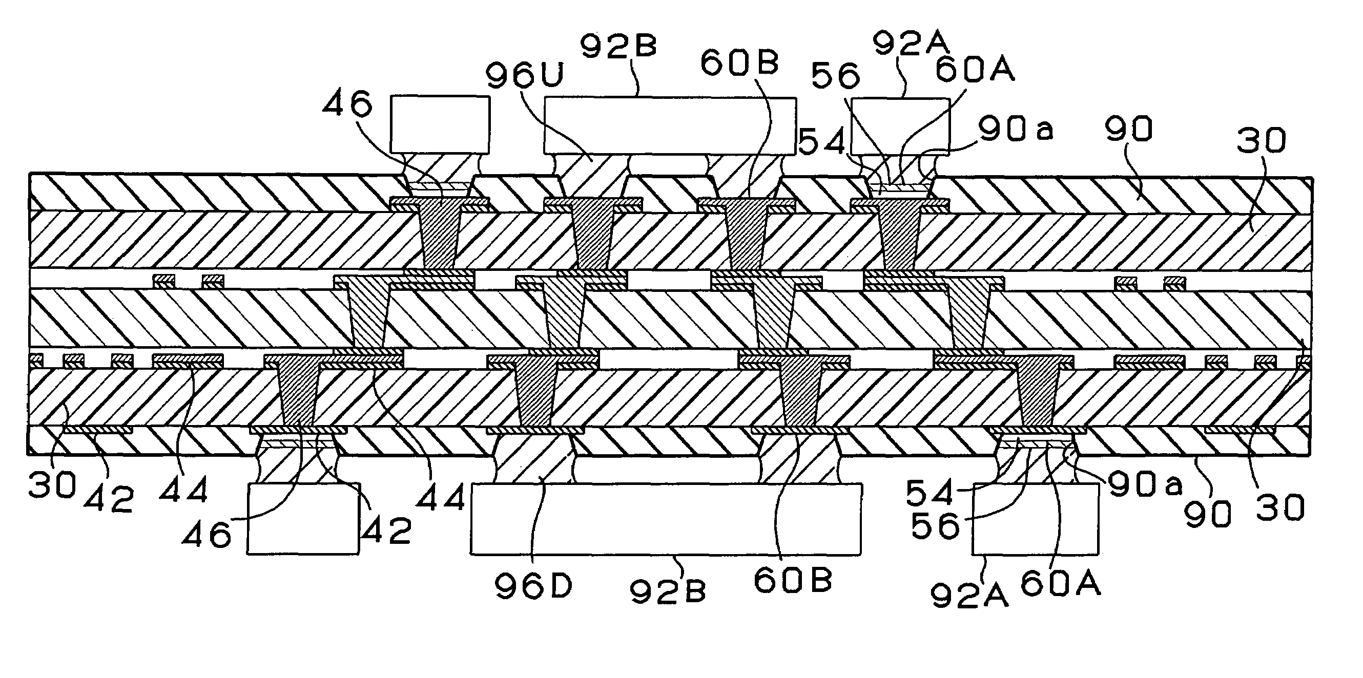
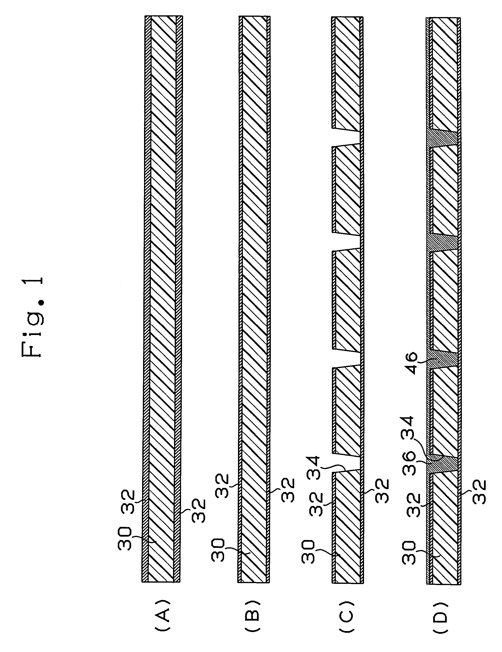
[0128](1) First, a double sided circuit board intended to constitute a multilayer circuit board is manufactured. This circuit board utilizes a double sided copper-clad lamination obtained by overlaying prepreg 30 as B-stage created by impregnating glass fabric with expoxy resin and copper foil 32 and pressing with heat as a starting material (FIG. 1(A)).

[0129]The thickness of this insulation base material was 75 μm and the thickness of the copper foil was 12 μm. It is permissible to use a copper foil thicker than 12 μm as this layered board and then adjust the thickness of the copper foil to 12 μm by etching treatment (FIG. 1(B)).

[0130](2) The copper foil 32 and the insulation base material 30 were drilled by irradiating the double sided circuit board having the copper foil 32 with carbon dioxide gas laser and a via hole formation opening 34 reaching the copper foil 32 on an opposite side was formed (FIG. 1(C)). Further, the desmear treatment was performed within the open...

example 1-2

[0157]This example is the same as the example 1-1 except that no OPS layer was formed on a solder pad in which the corrosion resistant layer of the example 1-1 is not formed.

example 1-3

[0158]This example is the same as the example 1-1 except that corrosion resistant layer of nickel-palladium-gold was formed on the solder pad in which the corrosion resistant layer of the example 1-1 was formed.


PUM

PropertyMeasurementUnit
temperatureaaaaaaaaaa
thicknessaaaaaaaaaa
thicknessaaaaaaaaaa

Abstract

This invention provides a multilayer printed wiring board in which electric connectivity and functionality are obtained by improving reliability and particularly, reliability to the drop test can be improved. No corrosion resistant layer is formed on a solder pad 60B on which a component is to be mounted so as to obtain flexibility. Thus, if an impact is received from outside when a related product is dropped, the impact can be buffered so as to protect any mounted component from being removed. On the other hand, land 60A in which the corrosion resistant layer is formed is unlikely to occur contact failure even if a carbon pillar constituting an operation key makes repeated contacts.

Description

BACKGROUND OF THE INVENTION[0001]1. Field of the Invention[0002]The present invention relates to a multilayer printed wiring board in which electronic components, semiconductor device and the like are mounted on the front face of a board thereof and a manufacturing method thereof and more particularly a multilayer printed wiring board preferably used for portable telephone, portable electronic appliance, electronic package and the like and a manufacturing method thereof.[0003]2. Description of the Related Art[0004]A unit of the circuit board is formed by drilling via holes in an insulation hard base material having a conductive circuit on at least one face and then forming conductive layer in their openings with metallic paste or plating. A multilayer circuit board (multilayer printed wiring board) can be obtained by preparing two or more pieces of these circuit boards and bonding those boards successively or collectively such that they are overlaid into multi-layers. At this time, ...

Claims


Application Information

Patent Timeline
Patent Type & Authority Patents(United States)
IPC IPC(8): H05K7/10
CPCH01L23/49816H05K1/113H05K3/243H01L23/49822Y10T29/49155H01L2224/16H01L2924/01004H01L2924/01025H01L2924/01046H01L2924/01078H01L2924/01079H01L2924/15174H01L2924/15311H01L2924/19105H01L2924/19106H05K1/114H05K3/28H05K3/282H05K3/4614H05K2201/0391H05K2201/10674H05K2203/0574H01L2924/01019H01L2924/01068H01L2224/16235Y10T29/49117Y10T29/49204Y10T29/49124Y10T29/49156Y10T29/49147H01L2924/00014H01L2924/00011H01L2224/0401H05K3/46H05K3/34
Inventor WATANABE, YASUHIROTAKAHASHI, MICHIMASAAOYAMA, MASAKAZUNAKAMURA, TAKENOBUYANAGISAWA, HIROYUKI
Owner IBIDEN CO LTD
Why Eureka
Try Eureka