System and method for illuminating a specimen with uniform angular and spatial distribution

a specimen and uniform angular and spatial distribution technology, applied in the field of illumination optics, can solve the problems of reducing sensitivity, coherent light may produce speckle and/or ringing in inspection images, and the performance requirements of inspection systems have increased over the years, so as to increase the numerical aperture

Active Publication Date: 2010-02-02
KLA TENCOR TECH CORP
View PDF9 Cites 20 Cited by
  • Summary
  • Abstract
  • Description
  • Claims
  • Application Information

AI Technical Summary

Benefits of technology

[0026]In one embodiment, the first cone may have a positive taper angle for converting light that enters the cone-shaped portion with high NA into lower NA. The third cone may have a substantially zero taper angle for preserving light that enters the cone-shaped portion with medium NA. The second cone may have a negative taper angle for converting light that enters the cone-shaped portion with low NA, as well as light converted to low NA by the positive taper angle, into higher NA. In particular, the negative taper angle may be adapted to increase the numerical aperture of substantially all light that enters the cone-shaped portion by ΔNA.

Problems solved by technology

However, the performance requirements of inspection systems has increased over the years, as a result of continually decreasing dimensions of the semiconductor devices.
One factor affecting the resolution and sensitivity of the inspection system is the quality of light used to illuminate the specimen or semiconductor wafer.
However, laser light sources generate coherent light, which is undesirable for inspection for many reasons.
For example, coherent light may produce speckle and / or ringing in the inspection images generated by the imaging sensor.
Ringing introduces artifacts into the inspection images, which reduce sensitivity and make it difficult to detect defects.
Any deviation from spatial or angular distribution uniformity will adversely affect the resolution and sensitivity of the inspection system, and therefore, is undesirable.
In addition to reducing detection resolution and sensitivity, the highly concentrated low NA light generated by illumination system 100 may create problems for high NA bright-field (BF) and dark-field (DF) inspection systems.
In particular, the highly concentrated low NA light may create light budget and lens damaging issues in such systems.

Method used


Image

  • System and method for illuminating a specimen with uniform angular and spatial distribution
  • System and method for illuminating a specimen with uniform angular and spatial distribution
  • System and method for illuminating a specimen with uniform angular and spatial distribution

Examples


Embodiment Construction

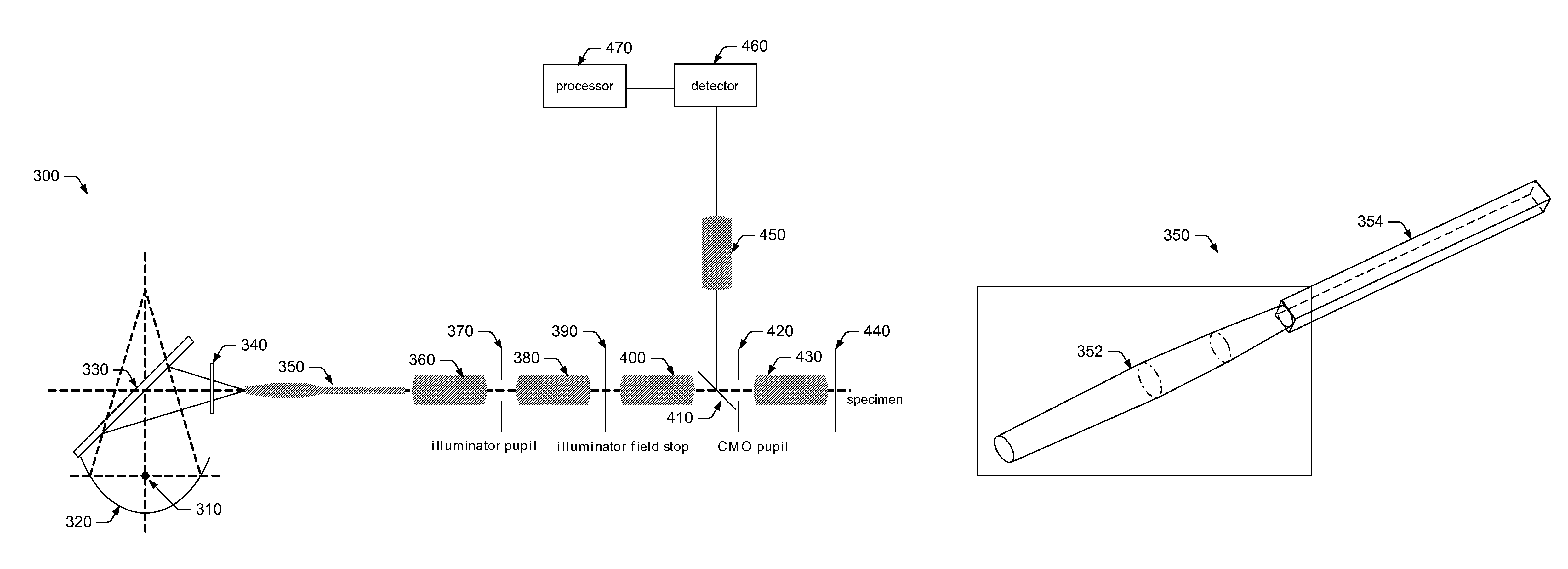
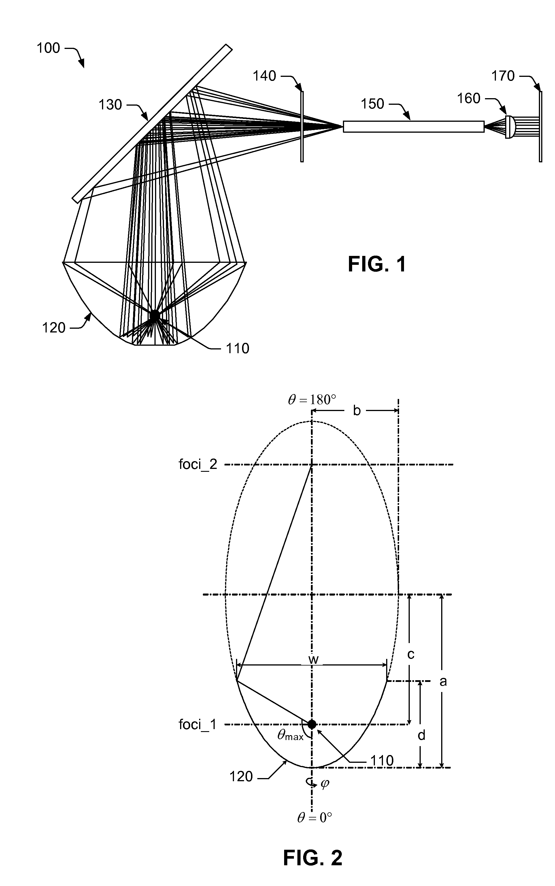
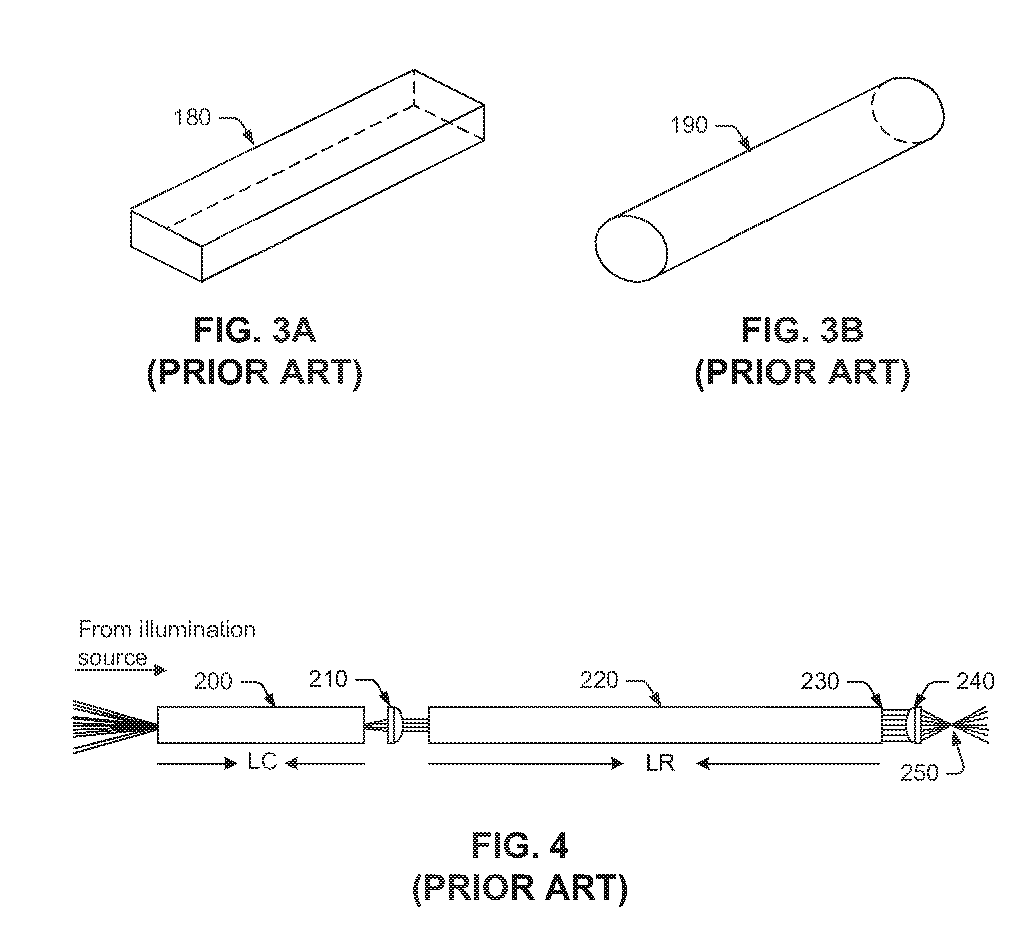
[0045]As used herein, the term specimen refers to a reticle or a wafer. The terms reticle and mask are used interchangeably herein. A reticle generally includes a transparent substrate such as glass, borosilicate glass, and fused silica having opaque regions formed thereon in a pattern. The opaque regions may be replaced by regions etched into the transparent substrate. Many different types of reticles are known in the art, and the term reticle as used herein is intended to encompass all types of reticles.

[0046]As used herein, the term wafer generally refers to substrates formed of a semiconductor or non-semiconductor material. Examples of such a semiconductor or non-semiconductor material include, but are not limited to, monocrystalline silicon, gallium arsenide, and indium phosphide. Such substrates may be commonly found and / or processed in semiconductor fabrication facilities.

[0047]A wafer may include one or more layers formed upon a substrate. For example, such layers may includ...


PUM


Abstract

A system for illuminating a specimen are disclosed herein. In general, the system may include an illumination source configured to generate light with an uneven distribution at a pupil plane and field stop of the system, a lightpipe coupled for redistributing the light across the pupil plane and field stop, and at least one optical element configured to direct the redistributed light onto a specimen. The lightpipe may generally include a cone-shaped portion and a rectangular-shaped portion. The cone-shaped portion is configured for modifying an angular distribution of the generated light, so that the redistributed light is uniformly distributed across the pupil plane of the system. The rectangular-shaped portion is formed contiguous with the cone-shaped portion and configured for modifying a spatial distribution of the generated light, so that the redistributed light is uniformly distributed across a field stop of the system. A method for illuminating a specimen and a system for inspecting a specimen are also disclosed herein.

Description

BACKGROUND OF THE INVENTION[0001]1. Field of the Invention[0002]This invention relates to illumination optics and, more particularly, to illumination pupil and field uniformity correction.[0003]2. Description of the Related Art[0004]The following descriptions and examples are given as background only.[0005]Fabricating semiconductor devices such as logic and memory devices typically includes processing a substrate using a large number of semiconductor fabrication processes to form various features and multiple levels of the semiconductor devices. For example, lithography is a semiconductor fabrication process that involves transferring a pattern from a reticle to a resist arranged on a semiconductor wafer. Additional examples of semiconductor fabrication processes include, but are not limited to, chemical-mechanical polishing, etch, deposition, and ion implantation. Multiple semiconductor devices may be fabricated in an arrangement on a single semiconductor wafer and then separated i...

Claims


Application Information

Patent Timeline
Patent Type & Authority Patents(United States)
IPC IPC(8): F21V33/00
CPCG01N21/8806G01N21/9501G02B6/0008G02B6/4298
Inventor CHEN, QIBIAOWANG, CHARLES N.
Owner KLA TENCOR TECH CORP
Why Eureka
Try Eureka