Method for measuring dimensions of sample and scanning electron microscope

a scanning electron microscope and sample technology, applied in material analysis using wave/particle radiation, instruments, nuclear engineering, etc., can solve the problems of deterioration of the characteristics of the device, change of the shape of the circuit pattern, and/or its destruction, so as to reduce the shrinkage of the pattern, accurate measurement of the dimension of the pattern, and accurate measurement of the pattern dimension

Inactive Publication Date: 2010-02-09
HITACHI LTD
View PDF22 Cites 17 Cited by
  • Summary
  • Abstract
  • Description
  • Claims
  • Application Information

AI Technical Summary

Benefits of technology

[0015]The first object of the present invention is to suppress the shrinkage of patterns, which are likely to suffer shrinkage due to electron beam irradiation during measurement, and thus to enable accurate dimension measurement of these patterns.
[0016]The second object of the present invention is to enable accurate measurement of pattern dimensions, irrespective of whether their shrinkage occurs.
[0017]In order to achieve the above-mentioned first object, by use of a scanning electron microscope equipped with an electron source, with a scanning means by which the surface of the sample placed on a sample mounting stage is to be scanned two-dimensionally using

Problems solved by technology

Through recent closer studies, however, it has come to be known that since the ArF laser beam is very brittle against electron beam irradiation, when a formed pattern is observed or measured using a scanning electron microscope, the acrylic resin and other components of the base material will suffer condensation reaction due to the convergent electron beam scan and the resulting decrease in volume (herei

Method used


Image

  • Method for measuring dimensions of sample and scanning electron microscope
  • Method for measuring dimensions of sample and scanning electron microscope
  • Method for measuring dimensions of sample and scanning electron microscope

Examples


embodiment 1

[0058]The shrinkage of the ArF photoresist pattern is likely to be caused by the chemical reaction due to the convergent electron beam entering the photoresist. The inventors have therefore performed experiments in order to empirically derive the relationship between the acceleration voltage Vacc to the pattern of the convergent electron beam, electron beam current density Ipd, and the amount of shrinkage. As a result, 2S (the amount of shrinkage at both edges of a linear pattern in the case that the amount of shrinkage at one edge is taken as S) has obeyed empirical formula (1).

2S=K1·VaccK2·{1-exp(−(Ipd0.5·n / K3))}  (1)

where 2S: the amount of shrinkage at both edges, Vacc: the acceleration voltage (V), K1, K2, K3: parameters determined by the photoresist, and n: the number of measuring operations. It can therefore be seen that to suppress the shrinkage of the ArF photoresist pattern, associated with the irradiation of the electron beam, it is effective to reduce the electron beam ir...

embodiment 2

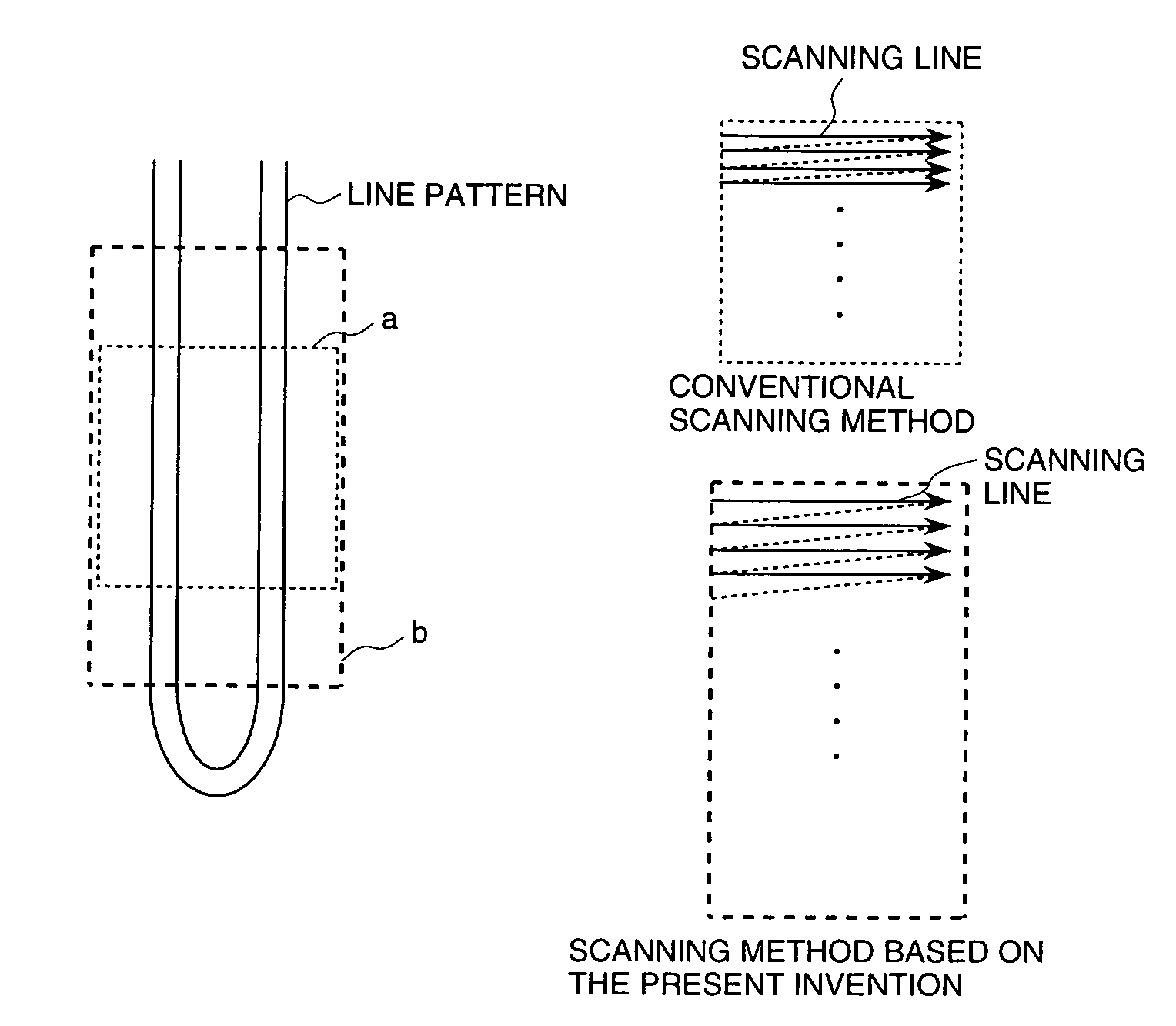
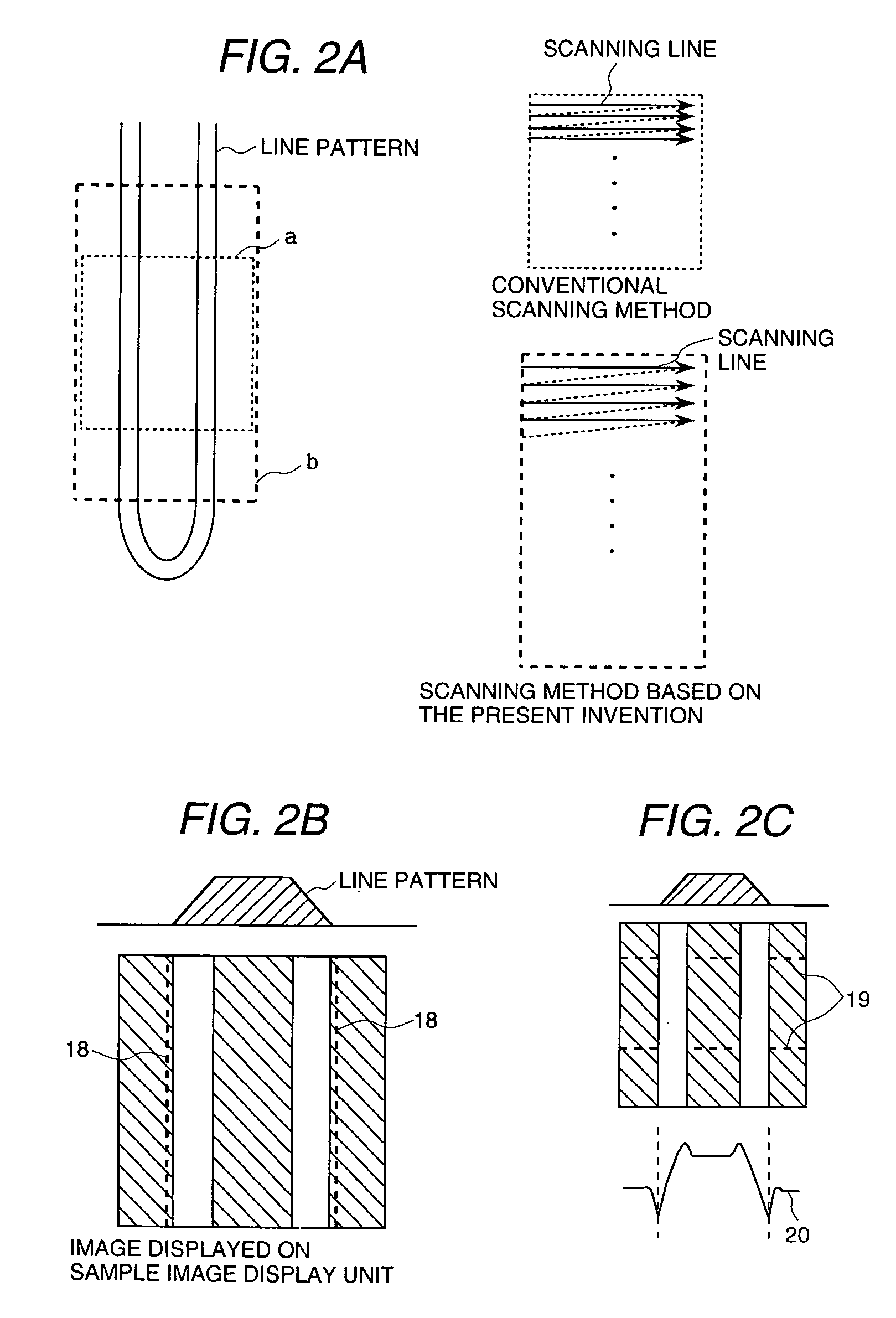
[0084]For a semiconductor device, in order to achieve its design performance, the shape and dimensions of its circuit pattern requires stringent management and for this purpose, a length-measuring electron microscope capable of measuring micro-dimensions is used during their inspection process. During observing and measuring processes, however, electron beam irradiation for length measurement changes the shape of the pattern, as shown in FIGS. 4 (1) to (3). If this pattern is a line pattern, the length value measured will be smaller than the dimension before it is measured, as shown in FIG. 8(a). If the pattern is a hole pattern, conversely, the length value measured will be larger than the dimension before it is measured, as shown in FIG. 8(b), and this will create the problem that the dimension existing before shrinkage occurs cannot be detected.

[0085]There is also the problem that when one section is continuously measured, since line width is varied by the repetition of electron ...


PUM


Abstract

The present invention suppresses decreases in the volumes of the patterns which have been formed on the surfaces of semiconductor samples or of the like, or performs accurate length measurements, irrespective of such decreases. In an electrically charged particle ray apparatus by which the line widths and other length data of the patterns formed on samples are to be measured by scanning the surface of each sample with electrically charged particle rays and detecting the secondary electrons released from the sample, the scanning line interval of said electrically charged particle rays is set so as not to exceed the irradiation density dictated by the physical characteristics of the sample. Or measured length data is calculated from prestored approximation functions.

Description

BACKGROUND OF THE INVENTION[0001]The present invention relates to a method of measuring the dimensions of microstructured patterns by use of a scanning electron microscope, and to the scanning electron microscope to be used for the above measurement; the invention relates more particularly to a method in which the dimensions of the samples varying in shape are to be measured by radiating electron beams, and to the scanning electron microscope to be used for the above measurement.[0002]During the manufacture and inspection of semiconductor devices, thin-film magnetic heads, and other functional element products by use of microstructured surface processing, scanning electron microscopes are commonly used to measure the widths of processed patterns (hereinafter, this measurement process is referred to as length measurement) and to visually inspect the patterns.[0003]The conventional scanning type of electron microscope is an apparatus intended to form images of samples, wherein the ele...

Claims


Application Information

Patent Timeline
IPC IPC(8): H01J37/28G01N23/225G01B15/00
CPCG01B15/00H01J37/28G01N23/225H01J2237/2814
Inventor NASU, OSAMUOTAKA, TADASHIKAWADA, HIROKIFUKAYA, RITSUOEZUMI, MAKOTO
Owner HITACHI LTD
Why Eureka
Try Eureka