Silicon-on-sapphire semiconductor device with shallow lightly-doped drain
a semiconductor and silicon-on-sapphire technology, applied in the field of semiconductor devices, can solve the problems of reducing battery life, increasing leakage current in the off-state, and particularly serious problems, and achieve the effect of suppressing current leakag
- Summary
- Abstract
- Description
- Claims
- Application Information
AI Technical Summary
Benefits of technology
Problems solved by technology
Method used
Image

Examples
first embodiment
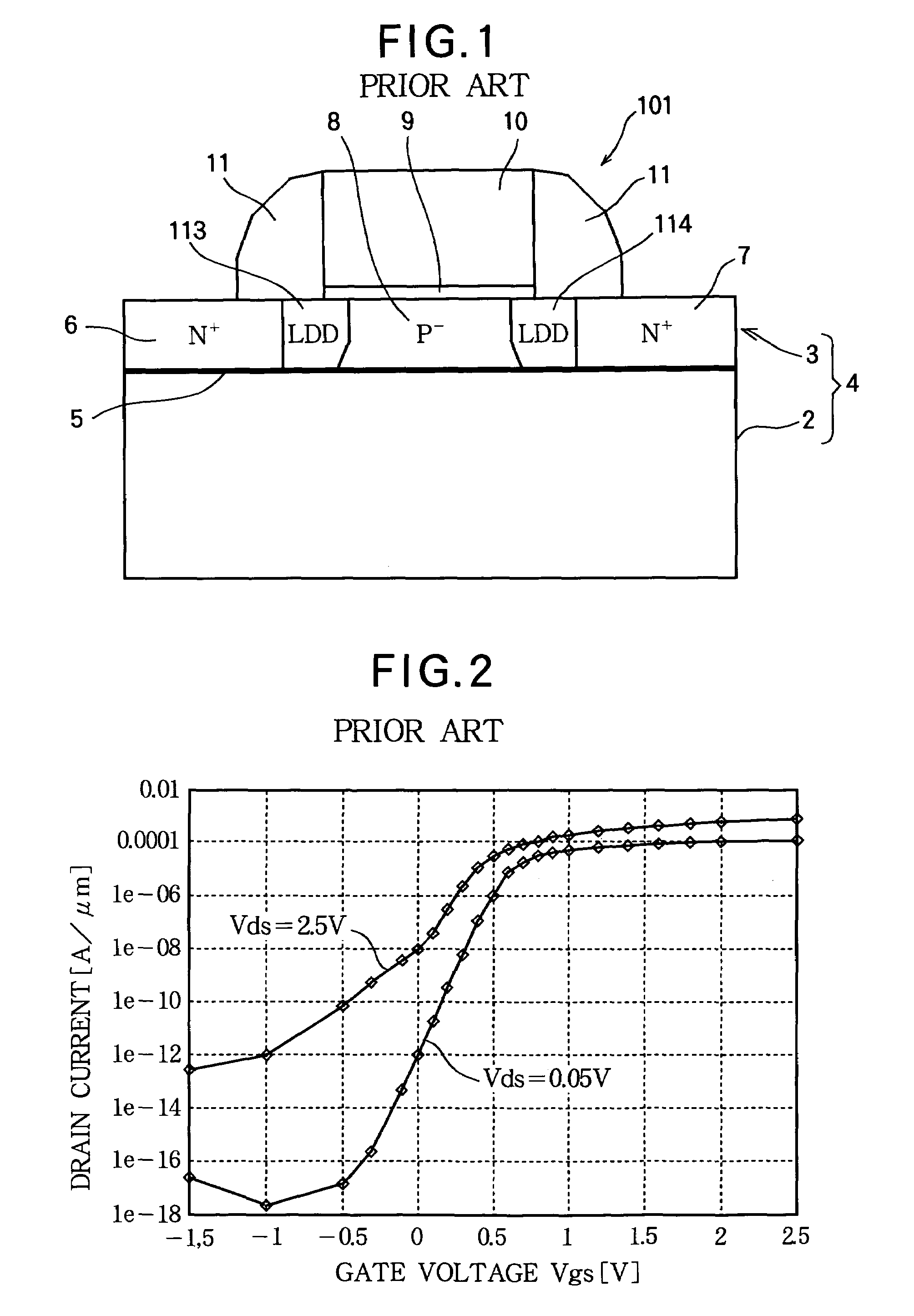
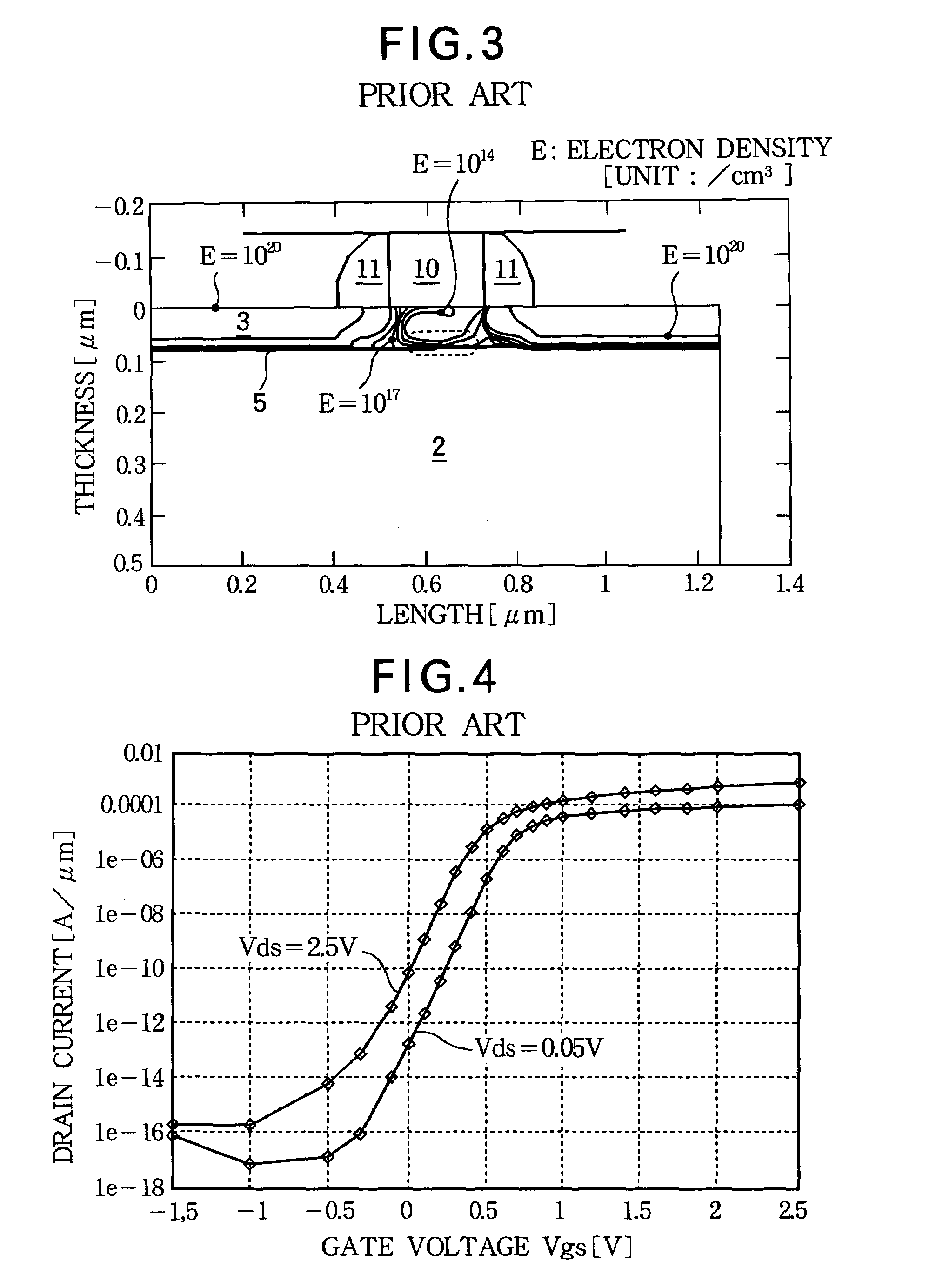
[0029]Referring to FIG. 5, the first embodiment is an nMOS device 1 having a sapphire substrate 2 and a thin silicon layer 3 formed on the sapphire substrate 2. The thickness of the silicon layer 3 is at most 0.1 μm; a thickness of 0.07 μm will be assumed below. The sapphire substrate 2 and silicon layer 3 constitute an SOS substrate 4. A source 6 and drain 7 are formed as n-type diffusions that reach the interface 5 between the silicon layer 3 and sapphire substrate 2. A p-type body region 8 occupies the space in the silicon layer 3 between the source 6 and drain 7. A gate oxide film 9 is formed on the body region 8, and a gate 10 is formed on the gate oxide film 9. A pair of side walls 11 are formed on the sides of the gate 10. The gate oxide film 9 and side walls 11 are formed as, for example, silicon oxide films. A lightly doped n-type diffusion layer or LDD layer 13 is formed in the body region 8 between the gate 10 and the source 6, adjoining one end of the source 6. Another L...
second embodiment
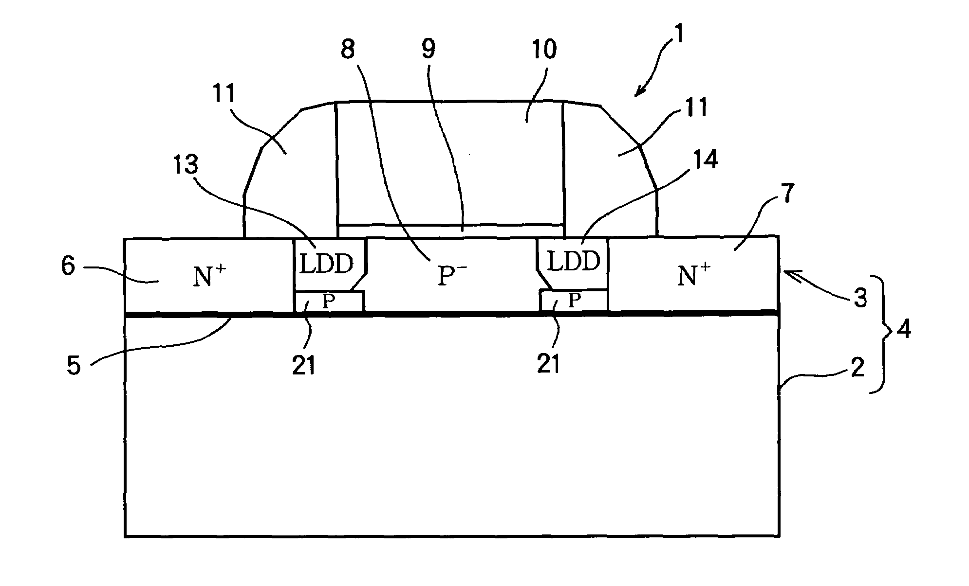
[0037]Referring to FIG. 8, the nMOS device 1 in the second embodiment is similar to the nMOS device in the first embodiment, but includes a pair of high-concentration diffusion layers 21, formed between the source LDD layer 13 and the interface 5 and between the drain LDD layer 14 and the interface 5, respectively. These diffusion layers 21 are doped with an impurity of same type (in this case, the p type) as the impurity in the body region 8, but at a higher concentration.
[0038]Being disposed below the LDD layers 13, 14, the high-concentration diffusion layers 21 do not impede the formation of a front channel extending between the LDD layers 13 and 14 in the on-state. They do, however, impede the formation of a back channel extending between the source 6 and drain 7 at the silicon-sapphire interface 5 in the off-state, because of the heightened concentration of the p-type impurity. More specifically, the high-concentration diffusion layer 21 beneath the LDD layer 14 inhibits the ex...
third embodiment
[0040]Referring to FIG. 9, the nMOS device 1 in the third embodiment is also similar to the nMOS device 1 in the first embodiment, but includes a high-concentration diffusion layer 21 doped with a p-type impurity at a higher concentration than in the body region 8, disposed between the source LDD layer 13 and the interface 5 and extending partly beyond the edge of the LDD layer 13 into the body region 8. The third embodiment is thus similar to the second embodiment, except that there is no high-concentration diffusion layer on the drain side, and the spatial extent of the high-concentration diffusion layer 21 on the source side is increased in compensation.
[0041]Being disposed at the silicon-sapphire interface 5, the high-concentration diffusion layer 21 in the third embodiment does not affect the formation of a front channel below the gate 10 in the on-state, but it does impede the formation of a back channel in the off-state. Essentially, the high-concentration diffusion layer 21 ...
PUM
 Abstract
Description
Claims
Application Information