
Electrostatic chuck

a technology of electrostatic chuck and chuck body, which is applied in the field of electrostatic chuck, can solve the problems of increased thermal contact resistance, hard ceramic insulating layer, and insufficient contact with wafers, and achieves improved cooling capacity, high accuracy, and high step accuracy

Inactive Publication Date: 2010-02-23
SHIN ETSU CHEM IND CO LTD
View PDF12 Cites 2 Cited by
  • Summary
  • Abstract
  • Description
  • Claims
  • Application Information

AI Technical Summary

Benefits of technology

The invention is an electrostatic chuck (ESC) that is used to hold wafers during semiconductor manufacturing processes. The ESC has an improved cooling capacity and minimizes particle generation. It allows for intimate contact with the wafer and maintains a uniform temperature, which is important for high accuracy processing. The ESC also allows for finer feature size processing and minimizes particle generation during wafer suction clamping.

Problems solved by technology

The ceramic insulating layer, however, is so hard that its contact with a wafer is not fully intimate because the wafer has an irregular surface.
This results in an increased thermal contact resistance and an insufficient cooling capacity.
This system, however, requires a fine working step of forming inert gas flow channels in the insulating layer surface and a feed source of the inert gas, and is disadvantageous in that the ESC structure becomes complex and the ESC manufacture cost is increased.
Physical contact and rub between the ceramic insulating layer and a wafer generate microscopic particles which deposit on the back side of the wafer so that they are carried over to the subsequent process, causing the problem of defects in the wafer microprocessing.
The electrostatic chuck using a polyimide insulating layer is easy to manufacture and inexpensive, but less durable against a plasma gas.
Undesirably it has a low heat conductivity and a high hardness which leads to an increased thermal contact resistance and an insufficient cooling capacity.
Like the ceramic insulator, it also suffers from the problem of particle generation.
However, a heat conductive filler such as alumina, zinc oxide or boron nitride which has been added to the silicone rubber for imparting heat conductivity thereto will escape and fall out, becoming particles.
While an ESC having minimal particle generation is needed to meet the current demand of reducing wafer processing line width toward higher integration, this ESC is regarded short in performance.
This ESC, however, has the risk that the contact improving layer itself can be transferred to the wafer or the heat conductive filler in the contact improving layer can fall out, causing particle generation.
This ESC, however, has the risk of particle generation because the heat conductive filler in the silicone rubber can fall out.
Where this protective film is hard, the wafer cooling capacity becomes low and rubs with a wafer can generate particles.
The filler other than silica in the protective film can fall out, causing particle generation.
Likewise, this ESC has the risk of particle generation from the tacky / anti-slip layer.

Method used

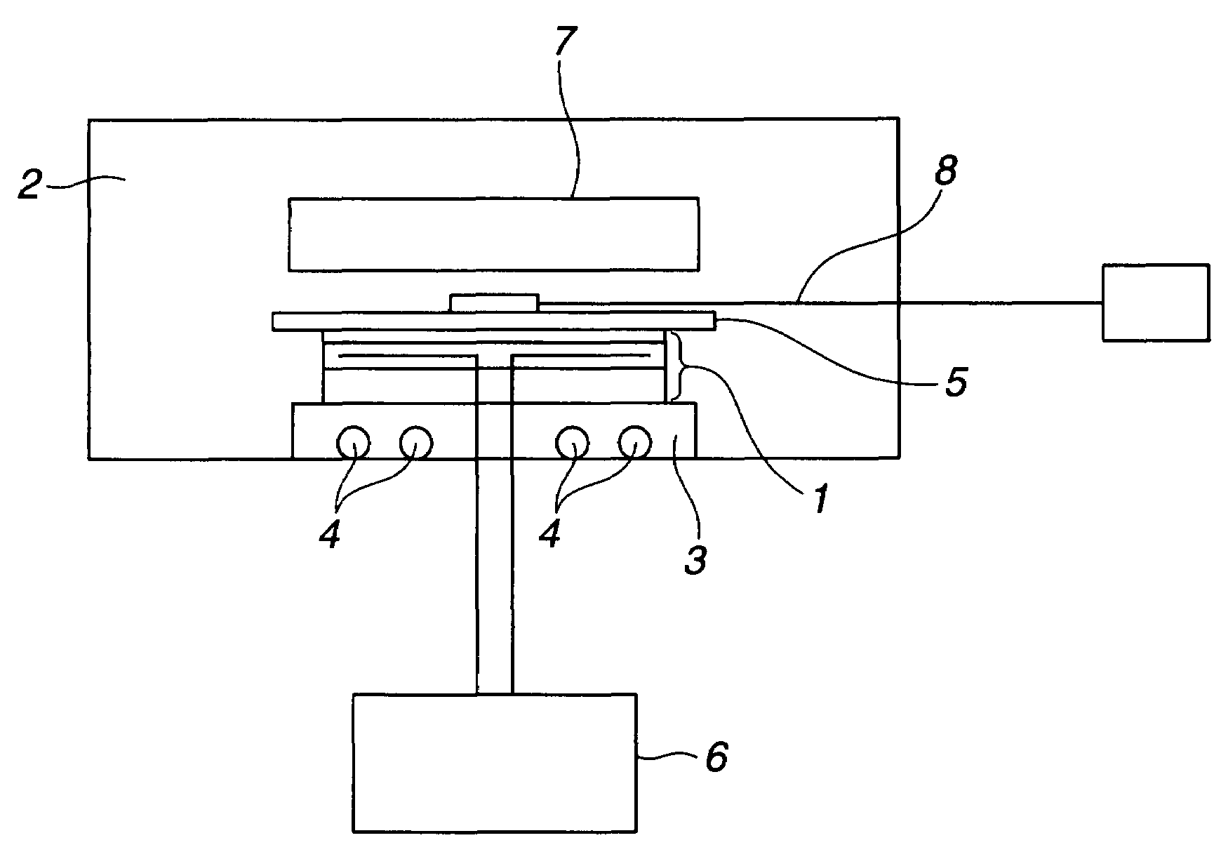
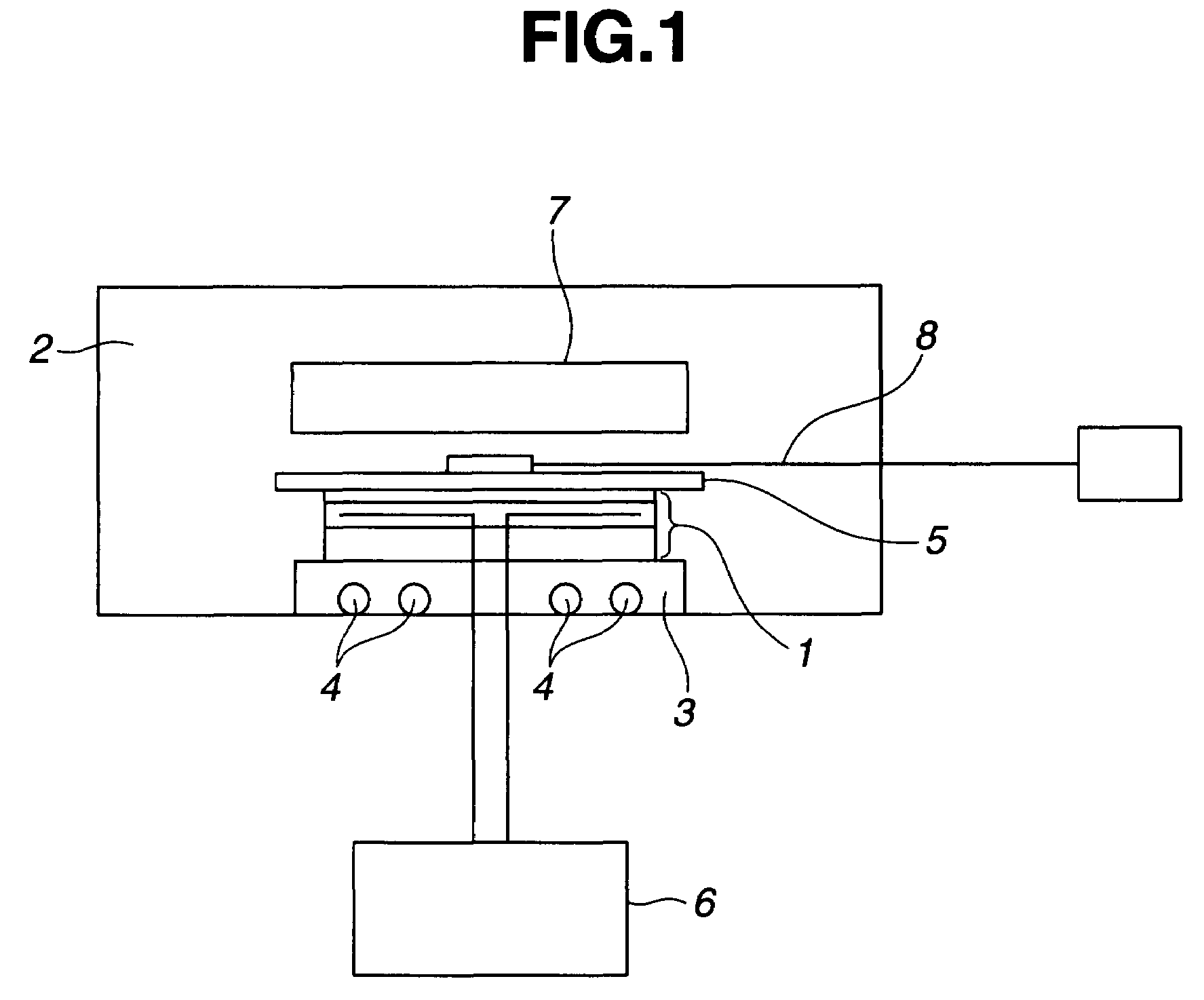

Image

  • Electrostatic chuck
  • Electrostatic chuck
  • Electrostatic chuck

Examples


example 1

[0036]Using a kneader, 100 parts by weight of methylvinylpolysiloxane consisting of 99.7 mol % dimethylsiloxane units and 0.3 mol % methylvinylsiloxane units and having an average degree of polymerization of 8,000 was kneaded with 65 parts by weight of fumed silica having a BET specific surface area of 300 m2 / g (Aerosil® 300 by Nippon Aerosil Co., Ltd.) and 15 parts by weight of dihydroxydimethylpolysiloxane of the structural formula (2). The mixture was heat treated at 170° C. for 3 hours.

[0037]

[0038]After cooling, the mixture was passed through a strainer with a 200-mesh metal screen for removing foreign matter. Using a two-roll mill, 0.7 part by weight of an organic peroxide, 2,5-dimethyl-2,5-di(t-butylperoxy)hexane was added and milled to form a reinforcing silica-filled silicone rubber composition. The filled silicone rubber composition, 100 parts by weight, was uniformly dissolved in 500 parts by weight of toluene on a homogenizer, and filtered through a 400-mesh metal screen,...

example 2

[0040]Using a kneader, 100 parts by weight of methylvinylpolysiloxane consisting of 99.85 mol % dimethylsiloxane units and 0.15 mol % methylvinylsiloxane units and having an average degree of polymerization of 8,000 was kneaded with 50 parts by weight of fumed silica having a BET specific surface area of 200 m2 / g (Aerosil® 1200 by Nippon Aerosil Co., Ltd.) and 8 parts by weight of dihydroxydimethylpolysiloxane of the structural formula (2). The mixture was heat treated at 170° C. for 3 hours. Using this reinforcing silica-filled silicone rubber composition, as in Example 1, a reinforcing silica-filled silicone rubber layer of 80 μm thick was formed on the surface of the polyimide ESC.

example 3

[0041]Using the reinforcing silica-filled silicone rubber composition in Example 1, a reinforcing silica-filled silicone rubber layer of 180 μm thick was similarly formed on the surface of the polyimide ESC.


PUM

PropertyMeasurementUnit
particle sizeaaaaaaaaaa
specific surface areaaaaaaaaaaa
thicknessaaaaaaaaaa

Abstract

An electrostatic chuck comprises an insulating layer with an electrode embedded therein and having a surface to come in contact with a workpiece to be held. Formed on the insulating layer surface is a silicone rubber layer which is filled with reinforcing silica, but free of another filler having an average particle size of at least 0.5 μm. The ESC allows for an intimate contact with a wafer and has an improved cooling capacity.

Description

CROSS-REFERENCE TO RELATED APPLICATION[0001]This non-provisional application claims priority under 35 U.S.C. §119(a) on Patent Application No. 2006-124971 filed in Japan on Apr. 28, 2006, the entire contents of which are hereby incorporated by reference.TECHNICAL FIELD[0002]This invention relates to an electrostatic chuck (ESC) useful in the manufacture of semiconductor integrated circuits, specifically in steps where wafers must be held in place, especially ion implantation, sputtering and plasma etching steps.BACKGROUND ART[0003]In the process of manufacturing semiconductor integrated circuits, wafers are usually held in place by wafer chucks of the electrostatic attraction or Johnsen-Rahbek effect type, that is, so-called electrostatic chucks. The electrostatic chuck includes an insulating layer, and organic resins such as polyimides, ceramics such as alumina and aluminum nitride, and rubber elastomers such as silicone rubber have been used as the insulating layer.[0004]In the pl...

Claims


Application Information

Patent Timeline
Patent Type & Authority Patents(United States)
IPC IPC(8): H01L21/683
CPCB32B15/08B32B15/20B32B25/08B32B25/20B32B27/06H01L21/6833B32B9/005B32B25/02B32B27/281B32B2264/102B32B2307/54B32B2457/14B32B27/36B32B2264/108B32B2307/206B32B2307/306B32B2307/3065B32B2457/08
Inventor NAKANO, AKIOHANDA, RYUICHISAKURAI, IKUO
Owner SHIN ETSU CHEM IND CO LTD
Learn More