Exposure apparatus and device manufacturing method using a common path interferometer to form an interference pattern and a processor to calculate optical characteristics of projection optics using the interference pattern

a technology of interferometer and manufacturing method, which is applied in the direction of measurement devices, instruments, photomechanical treatment, etc., can solve the problems of affecting the polarization state and affecting the polarization of the projection optics

Inactive Publication Date: 2010-03-09
CANON KK
View PDF11 Cites 13 Cited by
  • Summary
  • Abstract
  • Description
  • Claims
  • Application Information

AI Technical Summary

Benefits of technology

[0020]The present invention has been made on the basis of the recognition of the above problems, and has as its object to provide an exposure apparatus that has a function of measuring the optical characteristics of, e.g., projection optics at high speed and accurately.
[0024]The present invention can provide an exposure apparatus that comprises a function of measuring the optical characteristics of, e.g., projection optics at high speed and accurately.

Problems solved by technology

As the numerical aperture (NA) increases, the adverse influence of polarization becomes significant.
However, even by controlling the polarization of the exposure light by using an illumination system to achieve a desired polarization state, the polarization state in the projection optics can change due to distortion caused by holding a lens or by heating of the lens, use of a birefringent material, such as fluorite, and the like.
However, the above methods include various problems.
More specifically, with the above methods, the optical path is long and complicated, and not a common path, so the adverse influence of vibration is non-negligible.
In addition, generally, an exposure light source has a very short coherence length and is, accordingly, unsuited for measurement in an exposure apparatus.
It is impossible to measure retardation and azimuth, which are birefringence information of the optical system, simultaneously and accurately.
As retardation and azimuth of birefringence must be obtained accurately as aberration caused by polarization, the methods described above are not sufficient for this.
Since many of the methods require measurement light having a long coherence length, exposure light cannot be used as measurement light.
As the optical path is branched to cause interference between a reference wavefront and a detection surface, the interferometer is sensitive to vibration, requiring a long coherence length.
It is, therefore, very difficult to form such an interferometer arrangement in the exposure apparatus.
As described above, with only two linearly polarized light beams, the retardation and azimuth of birefringence cannot be calculated accurately.
In this case, although the retardation and azimuth of birefringence can be calculated, wavefront aberration cannot be calculated.
This increases the unit driving time and the measurement time, making it impossible to perform high-speed measurement.
This can increase the error.
Japanese Patent Laid-Open No. 2005-116732 does not disclose a method for this separate measurement.
As described above, the conventional methods cannot measure non-polarization aberration and polarization aberration (retardation and azimuth of birefringence) as the optical characteristics of the projection optics, simultaneously, at high speed and accurately, in the exposure apparatus.

Method used


Image

  • Exposure apparatus and device manufacturing method using a common path interferometer to form an interference pattern and a processor to calculate optical characteristics of projection optics using the interference pattern
  • Exposure apparatus and device manufacturing method using a common path interferometer to form an interference pattern and a processor to calculate optical characteristics of projection optics using the interference pattern
  • Exposure apparatus and device manufacturing method using a common path interferometer to form an interference pattern and a processor to calculate optical characteristics of projection optics using the interference pattern

Examples


first embodiment

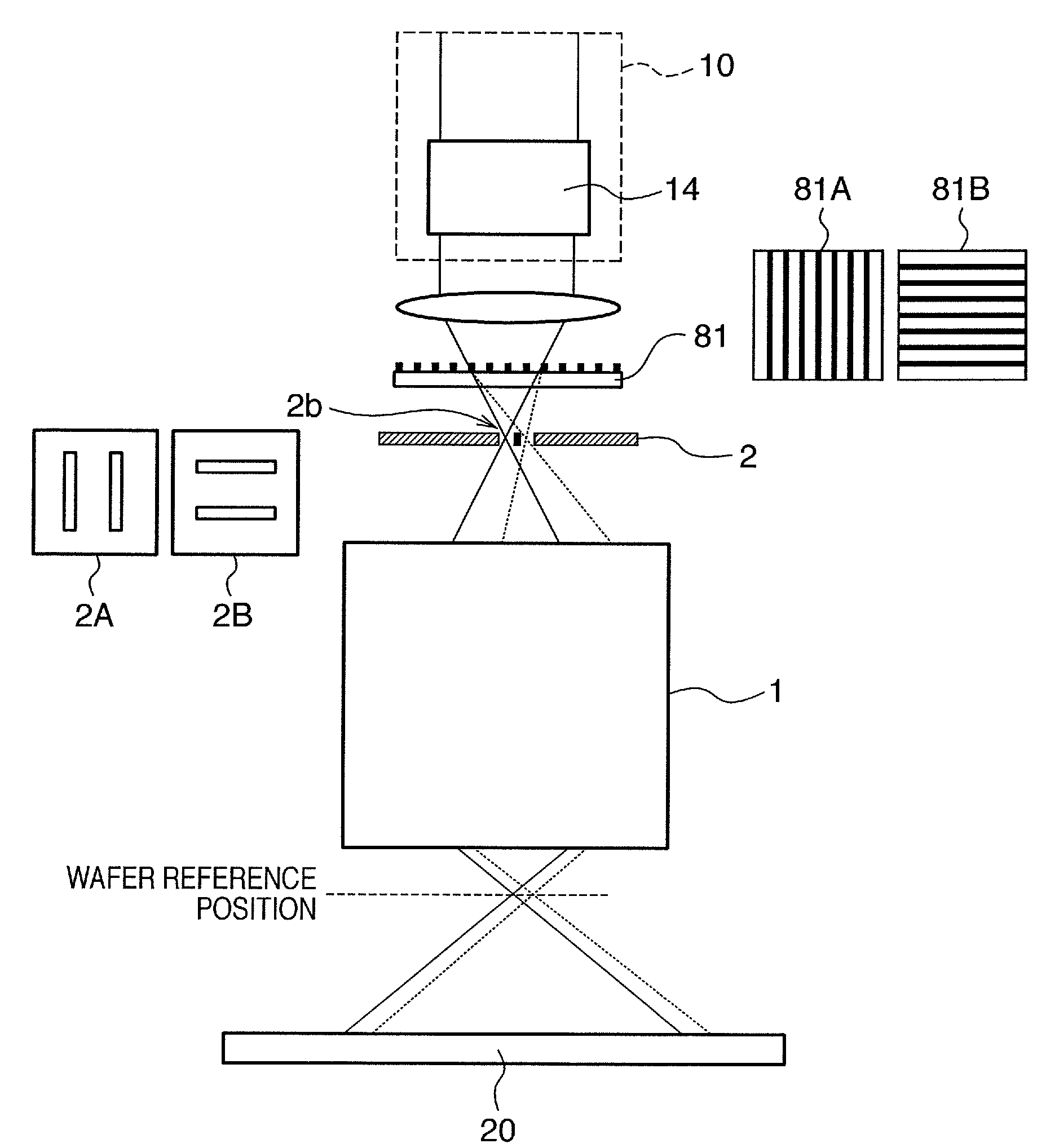
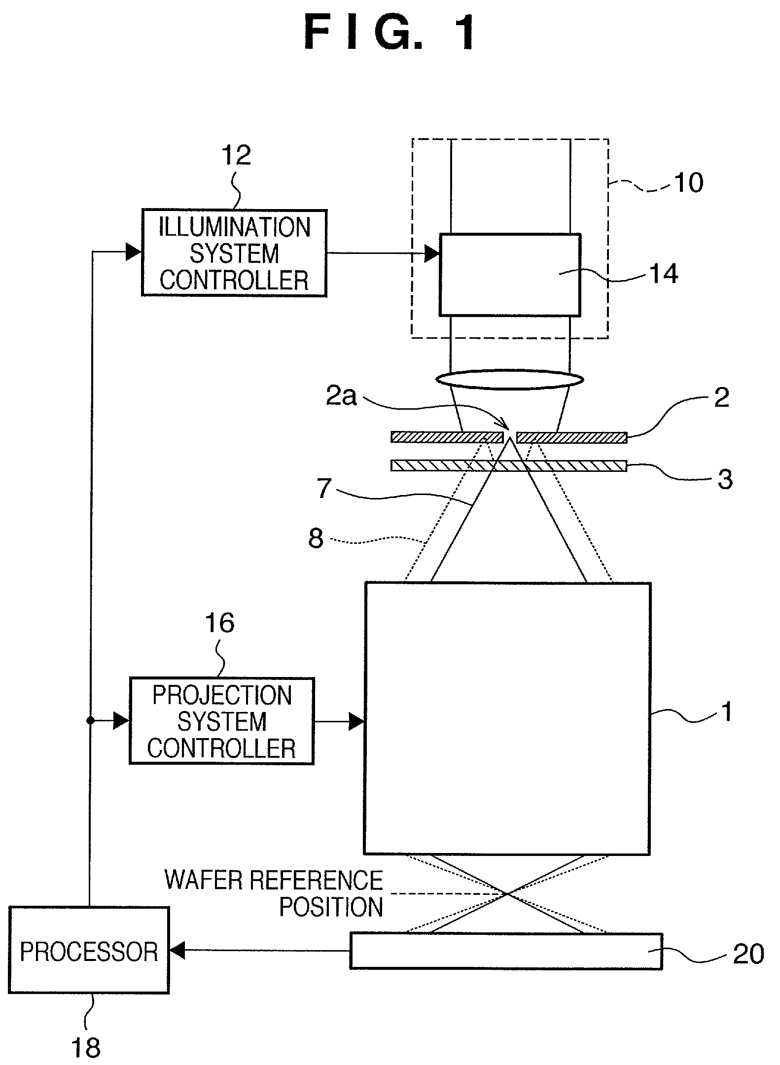
[0051]An exposure apparatus according to the first embodiment of the present invention will be described with reference to FIG. 1. The first embodiment provides an exposure apparatus that includes means for measuring non-polarization aberration and polarization aberration, which are the optical characteristics of the projection optics, using a radial shear interferometer (RSI). An example will be described in which, of the optical characteristics, aberration that does not depend on polarization is defined as non-polarization aberration and aberration that depends on polarization is defined as polarization aberration, and retardation and azimuth of birefringence are to be measured as polarization aberration.

[0052]In ordinary exposure, light provided by an illumination system 10 illuminates an exposure reticle (original), and the pattern of the reticle is projected onto a wafer (substrate) set at a wafer reference position through projection optics. The wafer reference position is ide...

second embodiment

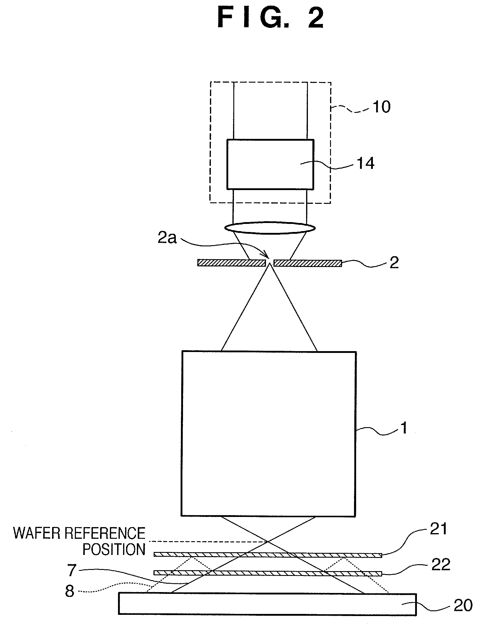
[0119]An exposure apparatus according to the second embodiment of the present invention will be described with reference to FIG. 2.

[0120]The second embodiment of the present invention provides another arrangement of the exposure apparatus that has a function of measuring non-polarization aberration and polarization aberration (retardation and azimuth), which are the optical characteristics of the projection optics, with a radial shear interferometer. An illumination system controller 12, a projection system controller 16, and a processor 18 are identical to their equivalents in the first embodiment.

[0121]In the second embodiment of the present invention, when measuring the wavefront of projection optics 1, a measurement reticle 2, having a pinhole 2a, is arranged at a reticle position, and first and second measurement substrates 21 and 22 are arranged between the projection optics 1 and an image sensor 20.

[0122]An ideal wavefront free from aberration at an illumination system 10 is ...

third embodiment

[0129]An exposure apparatus according to the third embodiment of the present invention will be described with reference to FIG. 3.

[0130]The third embodiment of the present invention provides an exposure apparatus in which a lateral shearing interferometer (LSI) measures non-polarization aberration and polarization aberration (retardation and azimuth), which are the optical characteristics of the projection optics. Since this lateral shearing interferometer is a common path interferometer, its optical path and arrangement are simple and little affected by the vibration of the exposure apparatus. An illumination system controller 12, a projection system controller 16, and a processor 18 are identical to their equivalents in the first embodiment.

[0131]In the third embodiment of the present invention, when measuring the wavefront of the projection optics 1, a measurement reticle 2, having a pinhole 2a, is arranged at a reticle position, and a two-dimensional diffraction grating 31 is ar...


PUM


Abstract

An exposure apparatus including an illumination system which illuminates an original, and projection optics which project a pattern of the original illuminated by the illumination system onto a substrate. The apparatus includes an interferometer which forms an interference pattern including aberration information on the projection optics using a polarized light beam emitted from the illumination system, in which the interferometer is a common path interferometer in which two light beams forming interference pattern pass along a path in the projection optics, and a processor which calculates optical characteristics of the projection optics on the basis of the interference pattern formed by the interferometer. The illumination system including a polarization controller which sequentially generates at least three difference polarized light beams with respective polarization states different from each other. The processor separates first aberration and second aberration from wavefront aberration represented by the interference patterns sequentially formed by the interferometer using the at least three different polarized light beams, by calculating a data of the interference patterns, the first aberration being aberration which does not change dependent on a polarization state of polarized light beam entering the projection optics. The second aberration is aberration which changes dependent on the polarization state of the polarized light beam entering the projection optics.

Description

[0001]This application claims the benefit of Japanese Patent Application No. 2006-247354, filed Sep. 12, 2006, and Japanese Patent Application No. 2007-176467, filed Jul. 4, 2007, which are hereby incorporated by reference herein in their entirety.BACKGROUND OF THE INVENTION[0002]1. Field of the Invention[0003]The present invention relates to an exposure apparatus and a device manufacturing method.[0004]2. Description of the Related Art[0005]In a lithography process to manufacture a device, such as a semiconductor device, an exposure apparatus is used to transfer a pattern on a reticle (original) onto a wafer (substrate) coated with a resist. As the density and degree of integration of integrated circuits increase, the exposure apparatus requires a higher resolution, and, accordingly, the wavelength of the exposure light becomes shorter. More specifically, as a light source for the exposure apparatus, a KrF excimer laser (wavelength: 248 nm) and an ArF excimer laser (193 nm) have be...

Claims


Application Information

Patent Timeline
Patent Type & Authority Patents(United States)
IPC IPC(8): G01B9/02
CPCG03F7/70566G03F7/706G02B27/0025G03F7/70191
Inventor OHSAKI, YUMIKOSAWADA, YASUHIROYAMAZOE, KENJITAKEUCHI, SEIJI
Owner CANON KK
Why Eureka
Try Eureka