Multiple magneto-resistance devices based on doped magnesium oxide

a technology of magnesium oxide and magneto-resistance devices, which is applied in the field of magnetic junction devices, can solve the problems of affecting the performance of the device, reducing the use signal (r), and highly non-trivial task of fabricating efficient semiconductor diodes in metal-oxide mtj stacks

Inactive Publication Date: 2010-03-16
VNK INNOVATION
View PDF10 Cites 34 Cited by
  • Summary
  • Abstract
  • Description
  • Claims
  • Application Information

AI Technical Summary

Problems solved by technology

For very thin barriers of thickness less then 1 nm, however, the useful signal (ΔR) decreases due to microscopic pinholes and other defects in the barrier as described in [2].
However, fabricating efficient semiconductor diodes within metal-oxide MTJ stacks is a highly non-trivial task.
Roughness of even one monolayer can significantly affect the performance of the device.
The need for atomically thin and atomically smooth metal layers imposes practical limitations on the use of such a double barrier device where the center electrode is a metal.
However, the performance of such devices is presently often impaired by defects relating to the problems of providing thin enough layers separating the magnetic layers.

Method used


Image

  • Multiple magneto-resistance devices based on doped magnesium oxide
  • Multiple magneto-resistance devices based on doped magnesium oxide
  • Multiple magneto-resistance devices based on doped magnesium oxide

Examples


second embodiment

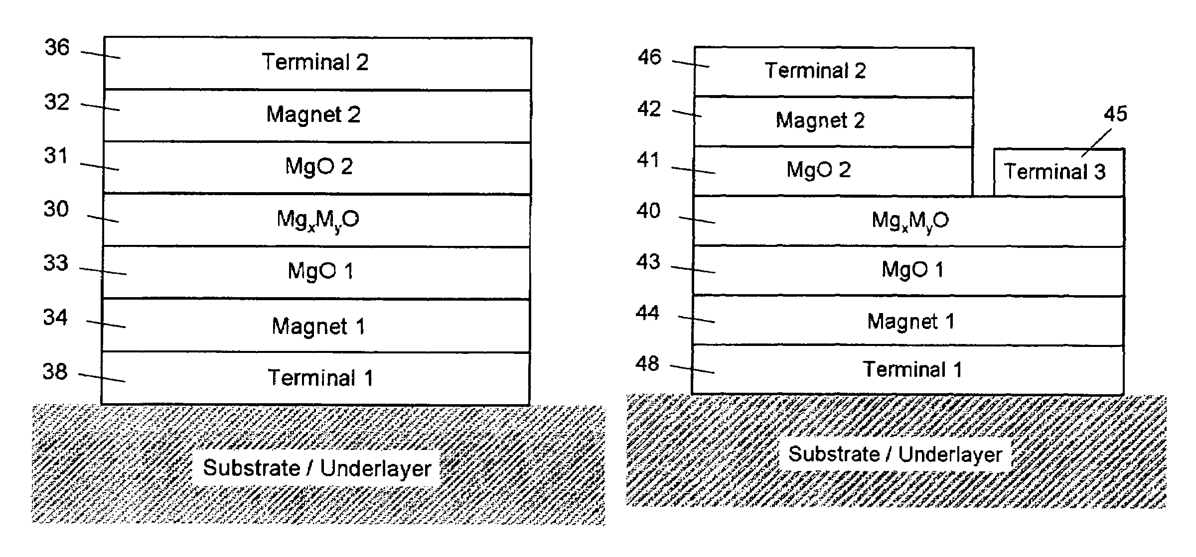
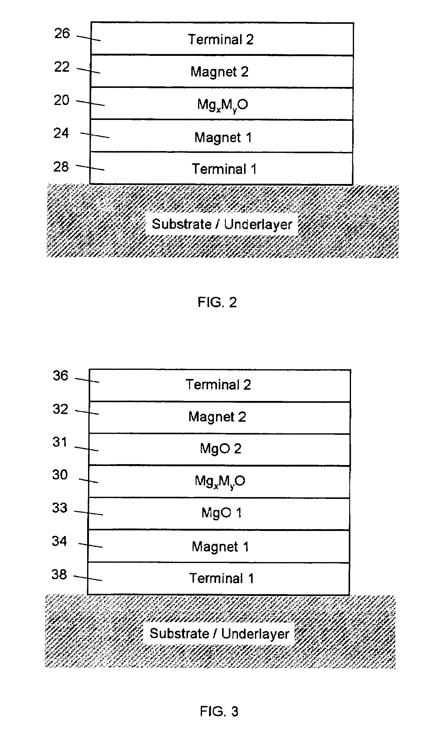
[0026]the present invention is a magnetic double junction as illustrated in FIG. 3, fabricated on a substrate or an underlayer generally as a part of an electronic circuit. Terminals 36 and 38 are connected to magnetic layers 32 and 34. The magnetic layers are preferably Fe, Co, Ni, alloys Fe—Co, Ni—Fe, Fe—Co—B, or other magnetic materials. The magnetic layers are insulated with MgO layers 31 and 33 from a layer of doped MgxMyO 30. Layers 30, 31, 33 are produced by post-deposition oxidation or reactive sputtering in Ar—O2 atmosphere of doped and pure Mg in the case of layer 30 and layers 31 and 33, respectively. The concentration of Mg in layer 30 is preferably x>0.9. The concentration of the metal dopant is y34, 33, 30, 31, 32. In addition to MR the device has diode functionality. The thicknesses of the two MgO barriers are individually varied from 20%) and the diode effect (preferably RR>10). Compared to the center metal layer in previous magnetic double junction devices the cente...

third embodiment

[0027]the present invention is a three terminal device as illustrated in FIG. 4, fabricated on a substrate or an underlayer generally as a part of an electronic circuit. Terminals 46 and 48 are connected to magnetic layers 42 and 44. The magnetic layers are preferably Fe, Co, Ni, alloys Fe—Co, Ni—Fe, Fe—Co—B, or other magnetic materials. The magnetic layers are insulated with MgO layers 41 and 43 from a layer of doped MgxMyO 40. Layers 40, 41, 43 are produced by post-deposition oxidation or reactive sputtering in Ar—O2 atmosphere of doped and pure Mg in the case of layer 40 and layers 41 and 43, respectively. The concentration of Mg in layer 40 is preferably x≧0.9. The concentration of the dopand is y44, 43, 40, 41, 42. Layers 42 and 46 are patterned in such a way as to allow a third terminal (45) be placed in contact with MgO layer 41. Changing the potential on this terminal affects through electrostatic fields the energy levels in layer 40 and thereby the resistance between termin...


PUM

PropertyMeasurementUnit
thicknessesaaaaaaaaaa
breakdown voltageaaaaaaaaaa

Abstract

The present invention provides a low resistance high magnetoresistance (MR) device comprised of a junction of two magnetic elements separated by a magnesium oxide (MgO) layer doped with such metals as Al and Li. Such device can be used as a sensor of magnetic field in magnetic recording or as a storage element in magnetic random access memory (MRAM). The invention provides a high-MR device possessing a diode function, comprised of a double junction of two outer magnetic elements separated by two MgO insulating layer and a center MgO layer doped with such metals as Al and Li. Such device provides design advantages when used as a storage element in MRAM. The invention with MR wherein a gate electrode is placed in electrical or physical contact to the center layer of the double tunnel junction.

Description

CROSS-REFERENCE TO RELATED APPLICATIONS[0001]This application is a National Stage application of PCT / SE2007 / 050078, filed Feb. 8, 2007, which claims priority from Swedish application SE 0600305-7, filed Feb. 10, 2006.FIELD OF THE INVENTION[0002]The present invention relates to magnetic field sensors, memory elements, and three-terminal logic devices for recording head, external field sensing, MRAM and logic applications. In particular the invention provides improved magnetic junction devices based on doped MgO layers.BACKGROUND OF THE INVENTION[0003]A device comprised of two ferromagnetic layers separated by an insulating tunnel barrier is known as a magnetic tunnel junction (MTJ). The cross-section of a conventional MTJ is illustrated in FIG. 1. It consists of bottom terminal 18 placed on a substrate or an underlayer, followed by the first magnetic layer 14, the oxide tunnel barrier 10, the second magnetic layer 12, and the top terminal 16. The resistance of such MTJ is a function ...

Claims


Application Information

Patent Timeline
Patent Type & Authority Patents(United States)
IPC IPC(8): H01L27/22H01L41/16H01L43/00
CPCB82Y25/00G01R33/093H01L43/08H01F10/3254G11C11/16G11C11/1659G11C11/161H10N50/10
Inventor KORENIVSKI, VLADISLAV
Owner VNK INNOVATION
Why Eureka
Try Eureka