

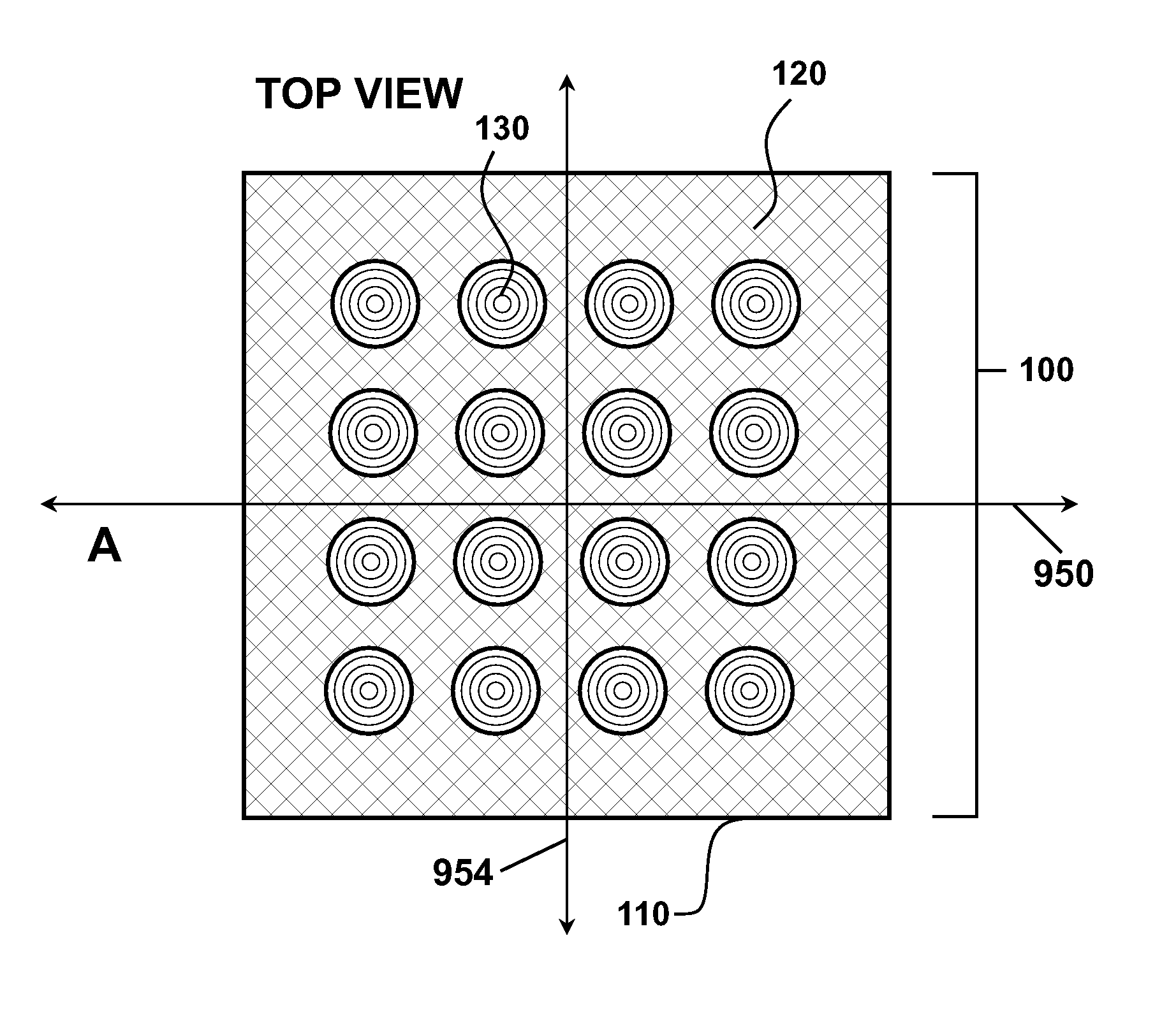
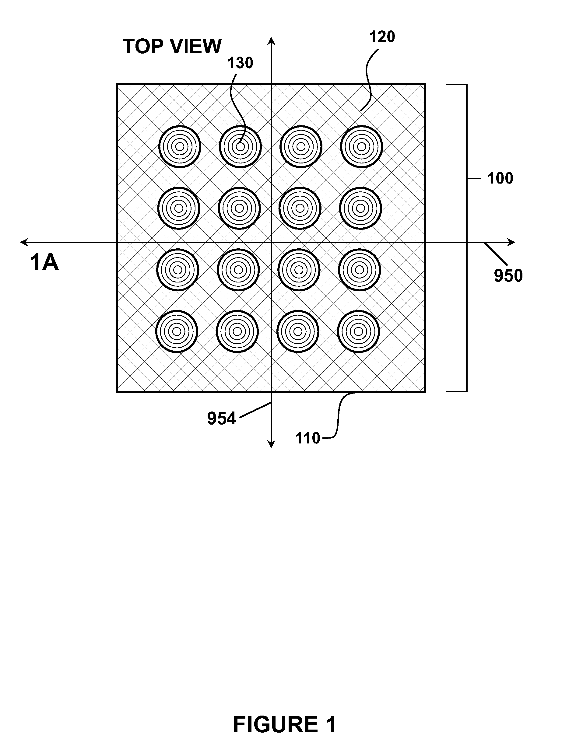
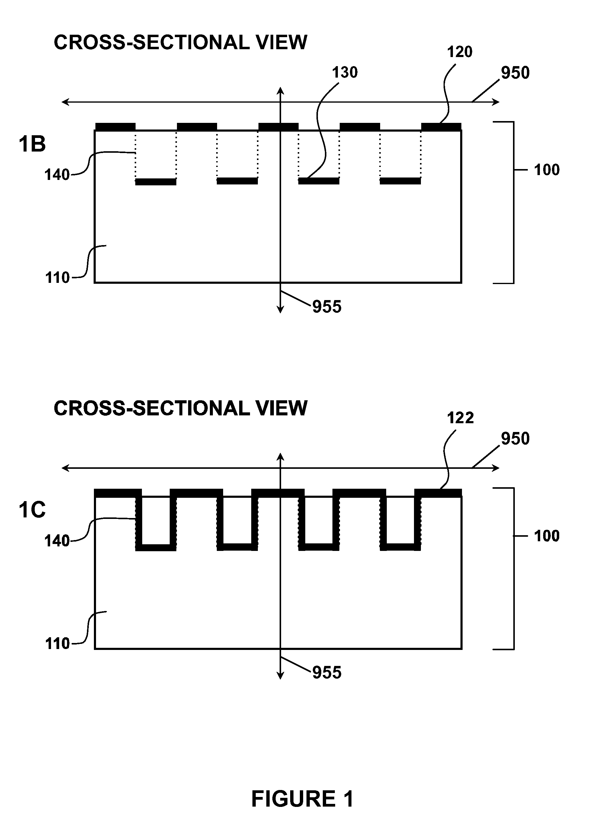
Multispectral plasmonic crystal sensors
a plasmonic crystal and sensor technology, applied in the field of multispectral plasmonic crystal sensor, can solve the problems of difficult integration of kretschmann spr optical configuration into complex form factor devices useful for high-end applications, subject to several practical limitations, etc., and achieve the effect of improving local plasmonic field distribution
- Summary
- Abstract
- Description
- Claims
- Application Information
AI Technical Summary
Benefits of technology
Problems solved by technology
Method used
Image

Examples
example 1
High Performance Plasmonic Crystal Sensor Formed by Soft Nanoimprint Lithography
Abstract
[0117]This Example describes a new type of plasmonic sensor fabricated by imprint lithography using a soft, elastomeric mold. Angle-dependent, zero-order transmission experiments demonstrate the sensing potential of this device, which uses a two dimensional plasmonic crystal. Full angle-dependent mapping shows that the sensitivity to surface chemical binding events reaches maxima near regions of the plasmonic Brillouin zone where the dispersion curves of multiple surface plasmon polariton modes converge. This behavior, together with the simple, low cost procedures for building the structures, demonstrates an important role for these devices in high performance chemical and biological sensing.
Introduction
[0118]The field of biosensing exploits many technologies that are optically based. While heavily dominated by spectroscopic protocols that employ fluorescence, label-less methods that exploit the ...
experiment & results
[0122]We performed zero-order transmission experiments in order to obtain the PBZ map of these structures. The scheme of the setup is presented in FIG. 5. The sample was fixed on a 2-axis rotation stage mounted inside of a UV-Vis-NIR spectrophotometer (Cary 5G). One axis turned the device to the required polar angle of incidence θ. The other rotated the sample around the Z axis (FIG. 5). This stage defines the direction for excitation and propagation of the plasmonic modes on the metal surface. The transmission spectra have a nominal spectral resolution of 1 nm, and are collected in a dual beam configuration to account for any intensity fluctuations in the light source.
[0123]PBZ maps were acquired by fixing the desired polar angle of incidence (θ) and recording a transmission spectrum over a predefined wavelength range. The angle θ was varied between 0° and 75° with incremented steps of 0.5°. Two main directions inside PBZ were mapped. One corresponded to the ┌-X direction (sample r...
example 2
Quantitative Multispectral Biosensing and Imaging Using 3D Plasmonic Crystals
Abstract
[0134]We have developed a class of three dimensional plasmonic crystal that consists of multi-layered, regular arrays of sub-wavelength metal nanostructures. When coupled with quantitative electrodynamics modeling of their optical response, these crystals enable full multi-wavelength spectroscopic detection of molecular binding events with sensitivities that correspond to small fractions of a monolayer. The high degree of spatial uniformity in the crystals, which are formed by a soft nanoimprint technique, provides the ability to image these binding events with micron spatial resolution. These features, together with compact form factors, low cost fabrication procedures, simple readout apparatus, and ability for direct integration into microfluidic networks and arrays, suggest promise for these devices in label free bioanalytical detection systems.
Background and Results
[0135]Macromolecular biologica...
PUM
| Property | Measurement | Unit |
|---|---|---|
| heights | aaaaa | aaaaa |
| distances | aaaaa | aaaaa |
| thicknesses | aaaaa | aaaaa |
Abstract
Description
Claims
Application Information