

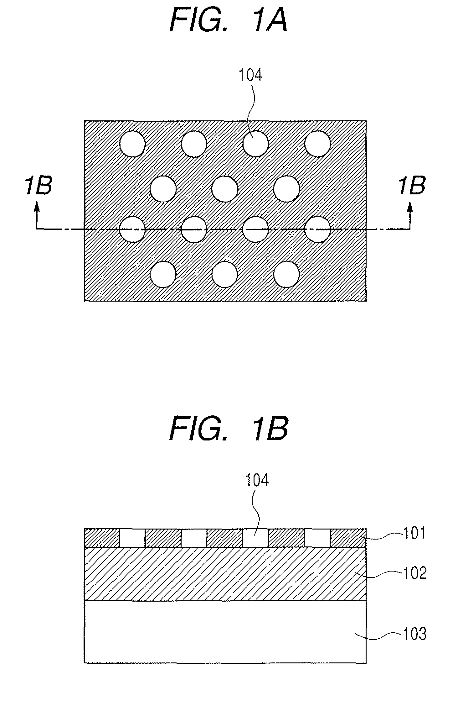
Photonic crystal and waveguide sensor device
a sensor device and waveguide technology, applied in the direction of optical radiation measurement, instruments, spectrometry/spectrophotometry/monochromators, etc., can solve the problems of deteriorating the quantitative accuracy of analysis, fluorescent labeling, and analysis method not yet practicably used in the true sens
- Summary
- Abstract
- Description
- Claims
- Application Information
AI Technical Summary
Benefits of technology
Problems solved by technology
Method used
Image

Examples
embodiment 1
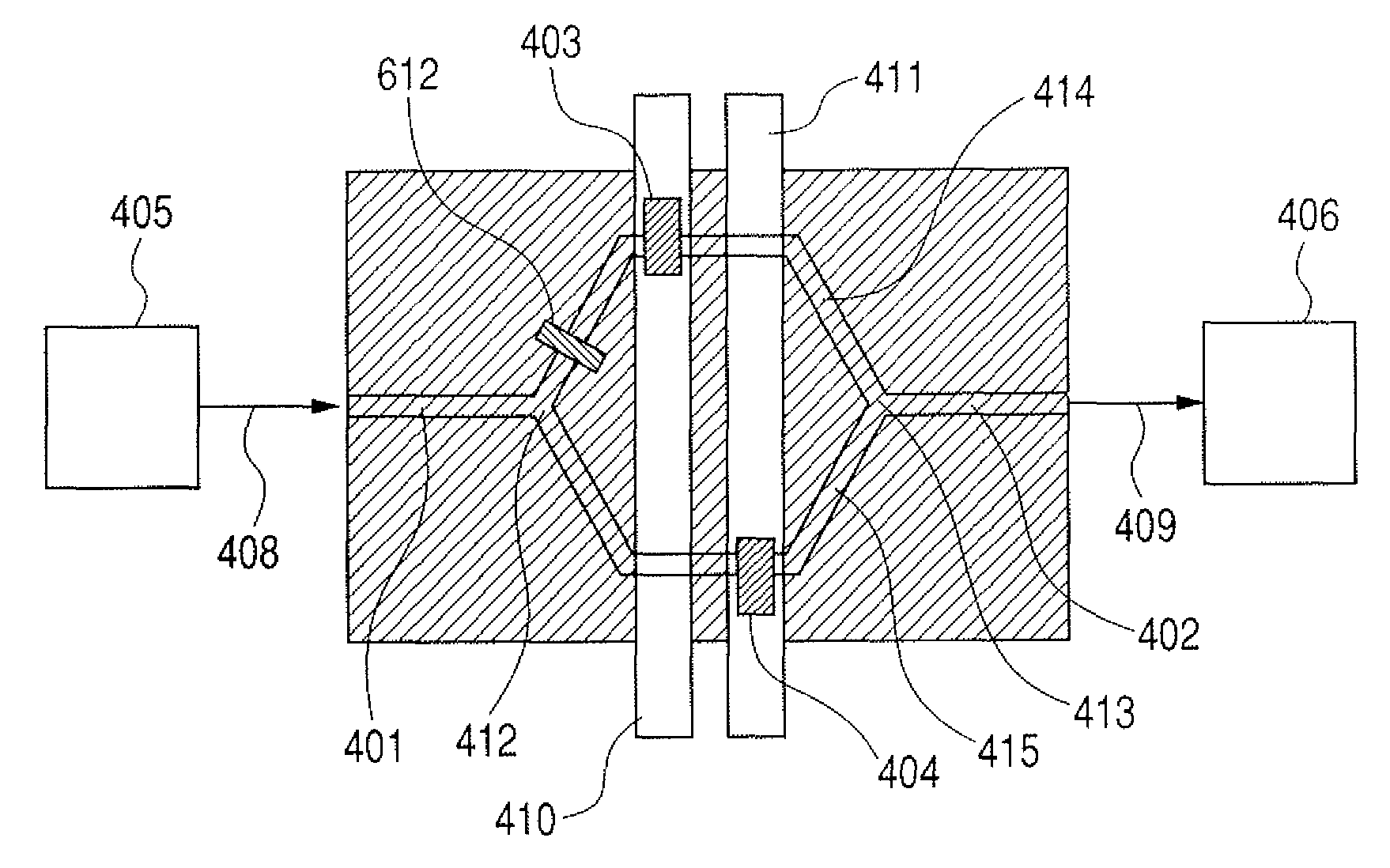
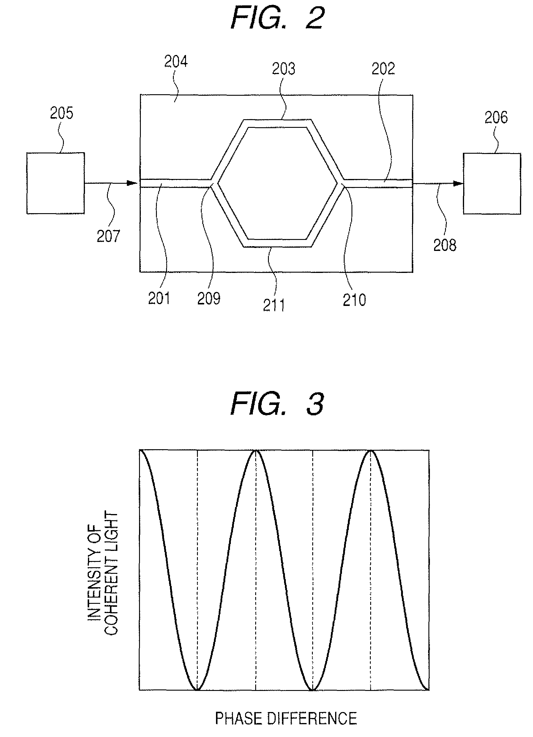
[0082]A sensor device in the present embodiment employs a Mach-Zehnder interferometer, and has a photonic crystal and a channel according to the present invention therein. The structure of the present embodiment will be now described with reference to FIG. 4 and FIGS. 5A to 5C.
[0083]The sensor device has two photonic crystals 403 and 404 arranged on a Mach-Zehnder interferometer composed of a substrate 407, a SiO2 layer 506 and a Si layer 503. Light 408 emitted from a light source 405 into an optical waveguide 401 is divided into two light waves at the first Y-branched waveguide 412, and each of the divided lights passes through a first photonic crystal 403 and an optical waveguide 414, and through a second photonic crystal 404 and an optical waveguide 415. Afterwards, they are synthesized to one at the second Y-branched waveguide 413, and the intensity of the light 409 emitted from the optical waveguide 402 is detected by a photo-detecting section 406. Specifically, each photonic c...
embodiment 2
[0090]The present embodiment shows one form of detecting synchronous light, while using a sensor device according to the present invention and a lock-in amplifier. A structure of the sensor device in the present embodiment will be now described with reference to FIG. 7.
[0091]A structure of the present embodiment employs a Mach-Zehnder interferometer similarly to the structure in Embodiment 1, but uses a synchronous detection system instead of measuring the intensity of interference light for a method for detecting the difference, which is a point different from the structure in Embodiment 1. The synchronous detection system is a procedure often used for removing noise. The sensor device has an optical switch 712 arranged in the first Y-branching part; makes the optical switch modulate incident light 408; synthesizes the lights having passed through photonic crystals 403 and 404 at the second Y-branched waveguide 413; makes a photo-detecting section 406 detect the light 409; and make...
embodiment 3
[0093]The present embodiment shows one form of a sensor device according to the present invention, which detects a refractive index of a fluid. The sensor device according to the present embodiment has the same structure as is shown in Embodiment 1 or 2, and detects the refractive index of the fluid flowing in a channel.
[0094]For instance, pass a fluid into a channel in the structure of a sensor device shown in FIG. 4. Specifically, pass the fluid having a refractive index to be detected into a channel 410 and a fluid having a known refractive index into a channel 411, and lights having passed through a photonic crystal 403 and a photonic crystal 404 cause a phase difference between them due to a difference between the refractive indexes of two fluids, and thereby the intensity of interference light changes. Then, when detecting the refractive index, take a procedure of estimating a quantity of a phase change from a quantity of change in the intensity of interference light, and esti...
PUM
| Property | Measurement | Unit |
|---|---|---|
| wavelength | aaaaa | aaaaa |
| wavelength | aaaaa | aaaaa |
| refractive index | aaaaa | aaaaa |
Abstract
Description
Claims
Application Information