Electro-optical device having an EL layer over a plurality of pixels

a technology of optical devices and el layers, applied in the direction of discharge tubes/lamp details, discharge tubes luminescnet screens, electric discharge lamps, etc., can solve the problems of enormous processing time of this method for forming the el layers corresponding to each pixel electrode, and achieve high thermal conductivity, prevent the transmission of alkali metals, and high heat radiating

Inactive Publication Date: 2010-06-29
SEMICON ENERGY LAB CO LTD
View PDF171 Cites 59 Cited by
  • Summary
  • Abstract
  • Description
  • Claims
  • Application Information

AI Technical Summary

Benefits of technology

[0010]The present invention aims to simplify the formation of an EL layer by an ink-jet method, and to perform high speed processing. An object of the present invention is to provide a method of manufacturing a high operation performance, high reliability electro-optical device, in particular a method of manufacturing an EL display device. In addition, an object of the present invention is to increase the quality of an electronic device having the EL display device as a display by increasing the picture quality of the electro-optical device.
[0012]A predetermined pattern is formed with the ink jet method by repeatedly performing positional control of an ink head and discharge of ink (when an EL layer is formed, a liquid containing the EL layer material). Note that if the screen size becomes large or the pixel density becomes high, then the amount of processing time by this method for forming the EL layers corresponding to each pixel electrode becomes enormous. However, with the above method of forming the stripe state or the oblong or rectangular shapes, it becomes possible to form the EL layers by continuously scanning the ink head and the amount of processing time can be shortened.
[0014]In addition, the diffusion of alkali metals from EL elements formed by the ink-jet method is prevented by an insulating film (passivation film) formed between the EL elements and TFTs with the present invention. Specifically, an insulating film for preventing transmission of alkali metals is formed on a leveling film covering the TFTs. In other words, a material may be used in which the diffusion speed of alkali metals throughout the insulating film at the operation temperature of the EL display device is sufficiently low.

Problems solved by technology

Note that if the screen size becomes large or the pixel density becomes high, then the amount of processing time by this method for forming the EL layers corresponding to each pixel electrode becomes enormous.

Method used


Image

  • Electro-optical device having an EL layer over a plurality of pixels
  • Electro-optical device having an EL layer over a plurality of pixels
  • Electro-optical device having an EL layer over a plurality of pixels

Examples


embodiment mode 1

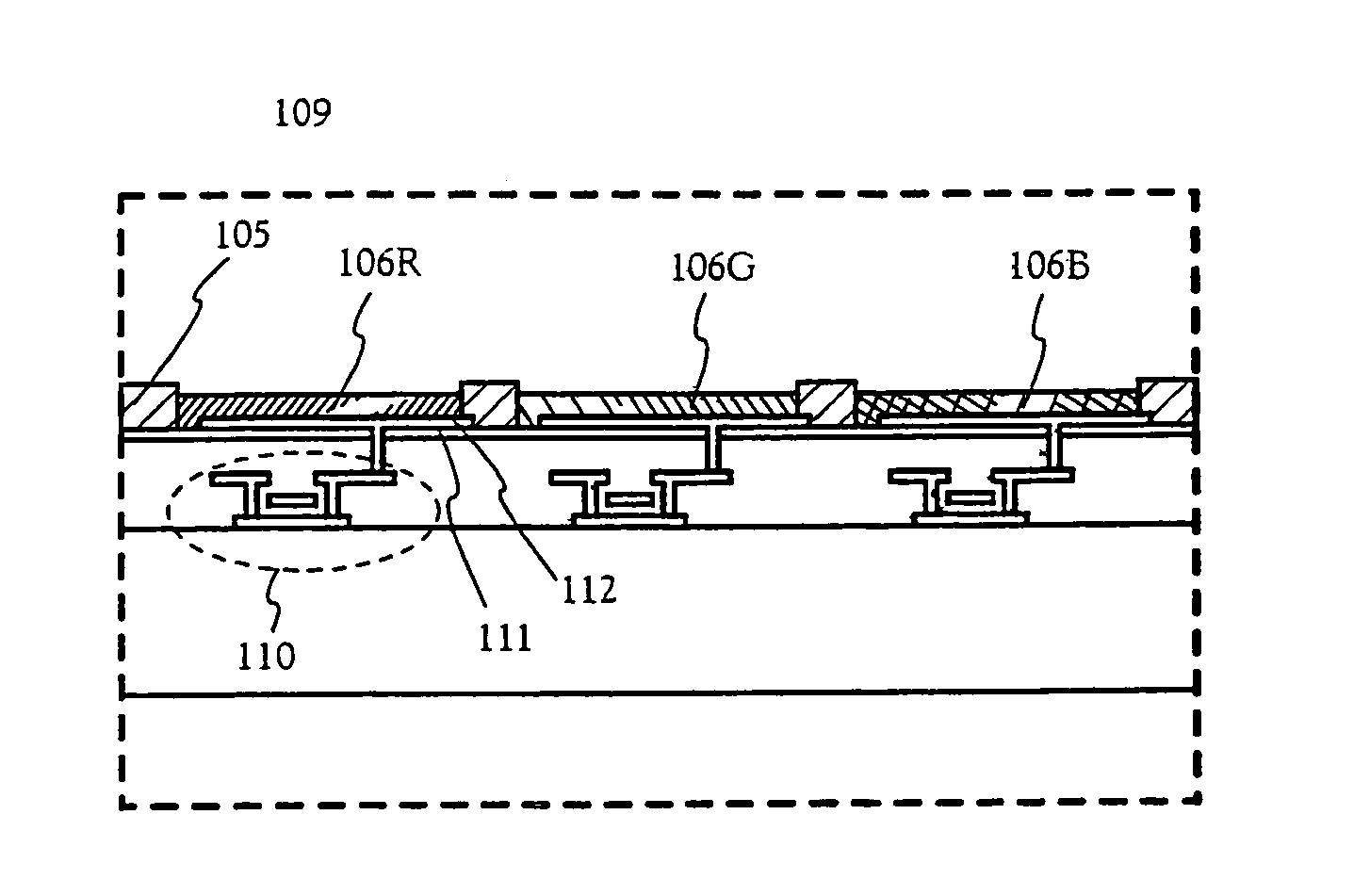
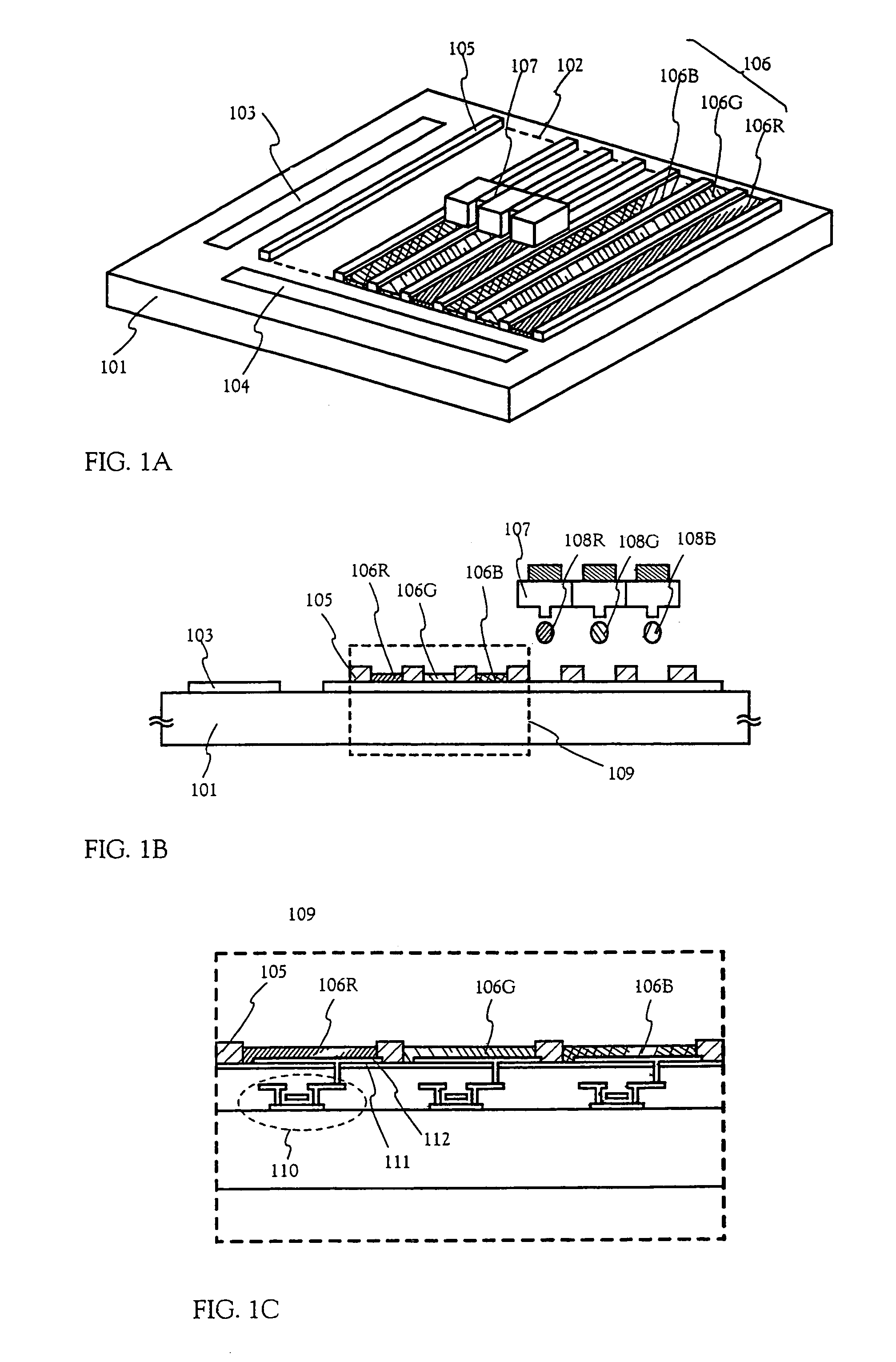
[0039]FIGS. 1A to 1C are diagrams for explaining the concept of the present invention. FIG. 1A shows a structure in which a pixel portion 102, a scanning line side driver circuit 103, and a data line side driver circuit 104 are formed on a substrate 101. Separation layers 105 are formed so as to form stripes in the pixel portion 102, and EL layers are formed between each separation layer. The separation layers 105 are formed in order that adjacent EL layers do not mutually mix when forming the EL layers by an ink-jet method.

[0040]EL layers 106 are formed by discharging a liquid containing an EL material from an ink head 107. There are no particular limitations on EL layer materials, but to perform color display EL layers 106R, 106G, and 106B may be formed corresponding to red, green, and blue, respectively.

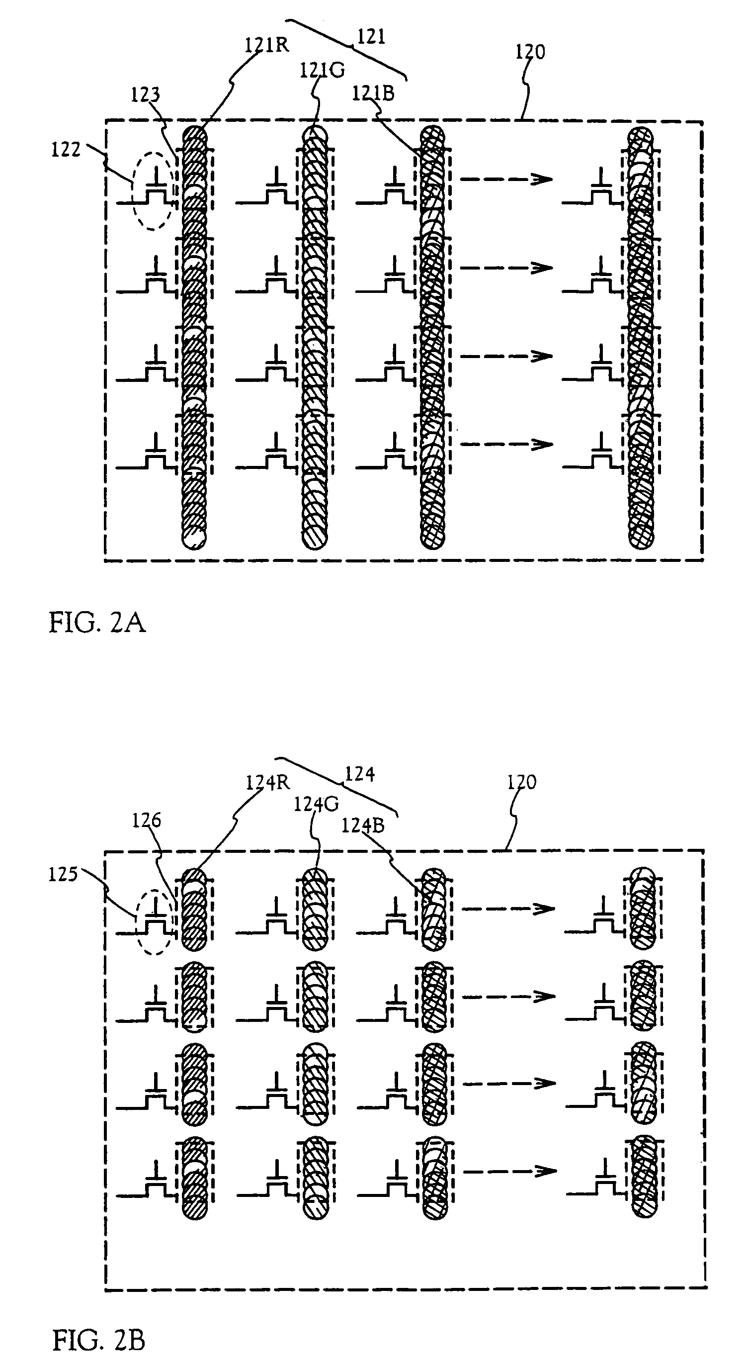
[0041]FIGS. 2A and 2B are diagrams for explaining details of the formation of the EL layers in the pixel portion. In FIG. 2A, a plurality of current control TFTs 122 and a plurali...

embodiment mode 2

[0047]An active matrix type EL display device of the present invention is explained with reference to FIGS. 5, 6A and 6B. Shown in FIG. 5 is a cross sectional diagram of a pixel of the active matrix type EL display device of the present invention, and FIG. 6A is a top view, and FIG. 6B is a circuit structure of the active matrix type EL display device. In practice, a plurality of these types of pixels are arranged in a matrix state, forming a pixel portion (image display portion).

[0048]Note that the cross sectional diagram of FIG. 5 shows a cross section cut along the line A-A′ in the top view shown in FIG. 6A. Common numerals are used in FIG. 5 and in FIGS. 6A and 6B, and therefore the three figures may be referenced as appropriate.

[0049]In FIG. 5, reference numeral 11 denotes a substrate, and reference numeral 12 denotes an insulating film serving as a base film. A glass substrate, a glass ceramic substrate, a quartz substrate, a silicon substrate, a ceramic substrate, a metallic ...

embodiment 1

[0120]The embodiments of the present invention are explained using FIGS. 7A to 9C. A method of simultaneous manufacture of a pixel portion, and TFTs of a driver circuit portion formed in the periphery of the pixel portion, is explained here. Note that in order to simplify the explanation, a CMOS circuit is shown as a basic circuit for the driver circuits.

[0121]First, as shown in FIG. 7A, a base film 301 is formed with a 300 nm thickness on a glass substrate 300. Silicon nitride oxide films are laminated as the base film 302 in embodiment 1. It is good to set the nitrogen concentration at between 10 and 25 wt % in the film contacting the glass substrate 300.

[0122]Besides, as a part of the base film 301, it is effective to provide an insulating film made of a material similar to the first passivation film 41 shown in FIG. 5. The current controlling TFT is apt to generate heat since a large current is made to flow, and it is effective to provide an insulating film having a heat radiati...


PUM


Abstract

The present invention aims to provide simple, high-speed processing for the formation of an EL layer by an ink-jet method. A method of manufacturing an electro-optical device having good operation performance and high reliability, and in particular, a method of manufacturing an EL display device, is provided. The present invention forms EL layers continuously across a plurality of pixels when the EL layers are formed by the ink-jet method. Specifically, with respect to m columns and n rows of pixel electrodes arranged in a matrix state, the EL layers are formed so as to form stripes with respect to one certain selected row or one column. The EL layers may also be formed having an oblong shape or a rectangular shape with respect to each pixel electrode.

Description

BACKGROUND OF THE INVENTION[0001]1. Field of the Invention[0002]The present invention relates to an electro-optical device typified by an EL (electroluminescence) display device formed by fabricating semiconductor elements (elements using a semiconductor thin film) on a surface of a substrate, and an electronic device including the electro-optical device as a display. Particularly, the invention relates to a method of manufacturing the same.[0003]2. Description of the Related Art[0004]In recent years, a technique for forming a thin film transistor (hereinafter referred to as a “TFT”) on a substrate has made remarkable progress, and its application and development to an active matrix type display device has proceeded. Especially, since a TFT using a semiconductor film that has a crystal structure (e.g., a polysilicon film) has a field effect mobility higher than a conventional TFT using an amorphous silicon film, a high speed operation can be made. Thus, it becomes possible to form a...

Claims


Application Information

Patent Timeline
Patent Type & Authority Patents(United States)
IPC IPC(8): H01J1/62H01L31/12H01L21/77H01L21/84H01L27/12H01L27/32H01L51/00H01L51/40H01L51/52H05B33/10H05B44/00
CPCH01L27/3244H01L27/3258H01L51/0005H01L27/12H01L27/1214H01L27/3211H01L51/524H01L51/5228H01L27/3246H01L29/78621H01L29/78624H01L29/78627H01L29/78645H10K59/35H10K59/124H10K59/122H10K71/135H10K59/80522H01L31/12H05B33/10H10K59/12H10K50/824H10K50/841
Inventor YAMAZAKI, SHUNPEIYAMAMOTO, KUNITAKAARAI, YASUYUKI
Owner SEMICON ENERGY LAB CO LTD
Why Eureka
Try Eureka