Nitride semiconductor laser element

a laser element and semiconductor technology, applied in the direction of lasers, semiconductor lasers, optical resonator shapes and construction, etc., can solve the problems of difficult to ensure the good performance of the laser element itself, the effect of diffraction grating still not satisfactory, and the difficulty of mass production and reproducibility, so as to increase the refractive index differential and lower the threshold current

Active Publication Date: 2010-08-24
NICHIA CORP
View PDF19 Cites 6 Cited by
  • Summary
  • Abstract
  • Description
  • Claims
  • Application Information

AI Technical Summary

Benefits of technology

[0012]The present invention was conceived in light of the above problems, and it is an object thereof to provide a nitride semiconductor laser element that has a simple constitution and does not entail any complication processing or the like, so that the refractive index differential can be effectively increased in the diffraction grating, and the threshold current can be lowered.
[0015]According to the nitride semiconductor laser element of the present invention, it is possible to increase the refractive index differential in the diffraction grating, and to lower the threshold current.

Problems solved by technology

With DFB laser diodes proposed in the past, however, the effect of the diffraction grating was still not satisfactory.
To this end, it is possible to obtain a refractive index differential by increasing the depth of the recessed and raised portions of the diffraction grating, but this poses problems in terms of mass production and reproducibility.
Also, even if these recessed and raised portions can be formed, when a semiconductor is regrown over this diffraction grating, there is a problem in that recessed and raised portions are produced on the growth surface, and it is difficult to ensure good performance of the laser element itself.

Method used


Image

  • Nitride semiconductor laser element
  • Nitride semiconductor laser element
  • Nitride semiconductor laser element

Examples


example 1

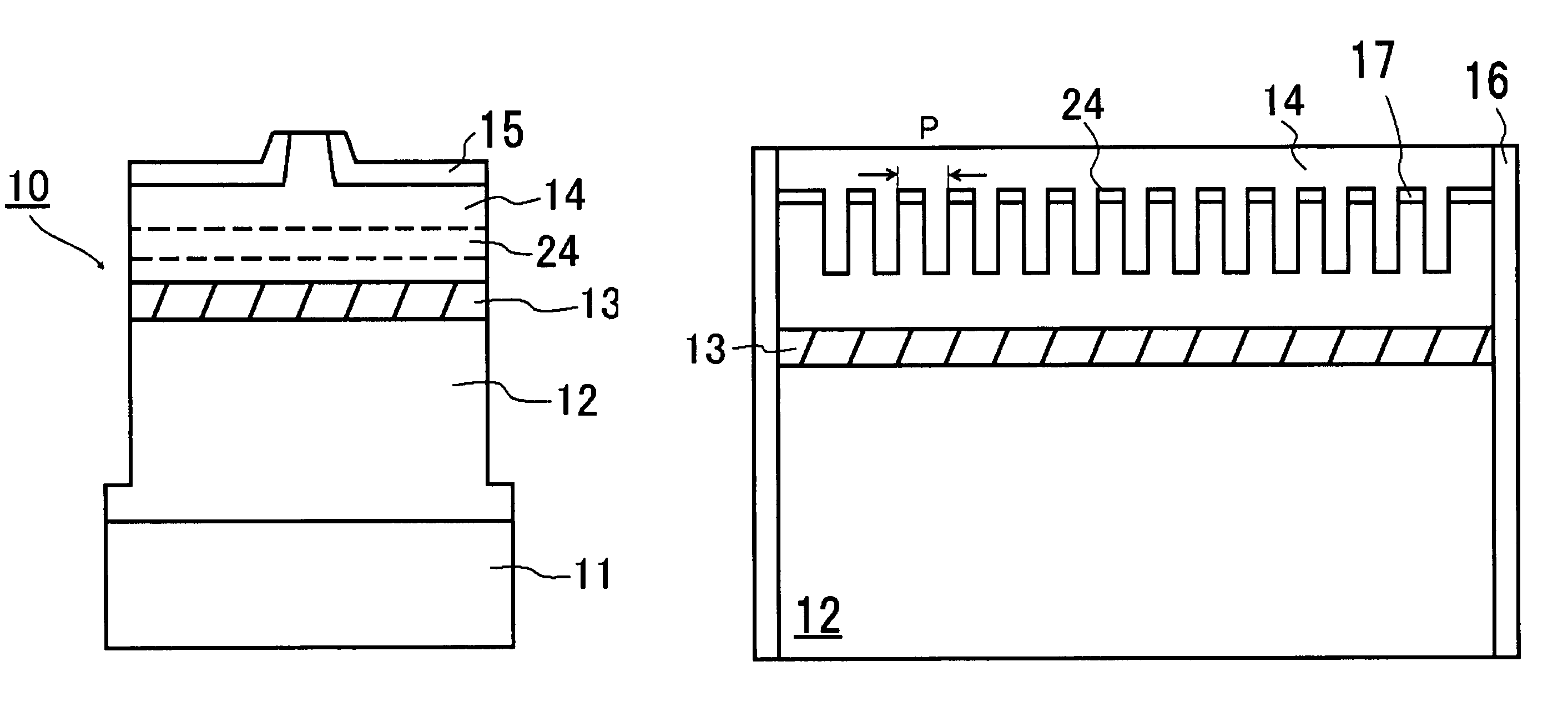
[0085]As shown in FIG. 1a, for example, the nitride semiconductor laser element comprises a substrate 11, a first semiconductor layer 12 (such as an n-type), an active layer 13, and a second semiconductor layer 14 (such as a p-type). This laser element further comprises a first electrode (not shown) and a second electrode (not shown) that are electrically connected to the first semiconductor layer 12 and the second semiconductor layer 14, respectively, a first protective layer (insulator) 15 is formed on the second semiconductor layer 14, and a second protective layer 16 (see FIG. 1b) is formed on a cavity facet.

[0086]A different type of substrate, composed of sapphire, is used as the substrate 11, and an under layer produced by lateral growth is formed on this via a buffer layer (not shown).

[0087]The compositions and thicknesses of the first semiconductor layer 12, the active layer 13 and the second semiconductor layer 14 are shown in Table 1.

[0088]

TABLE 1p-Contact LayerGaN: 15 nm ...

example 2

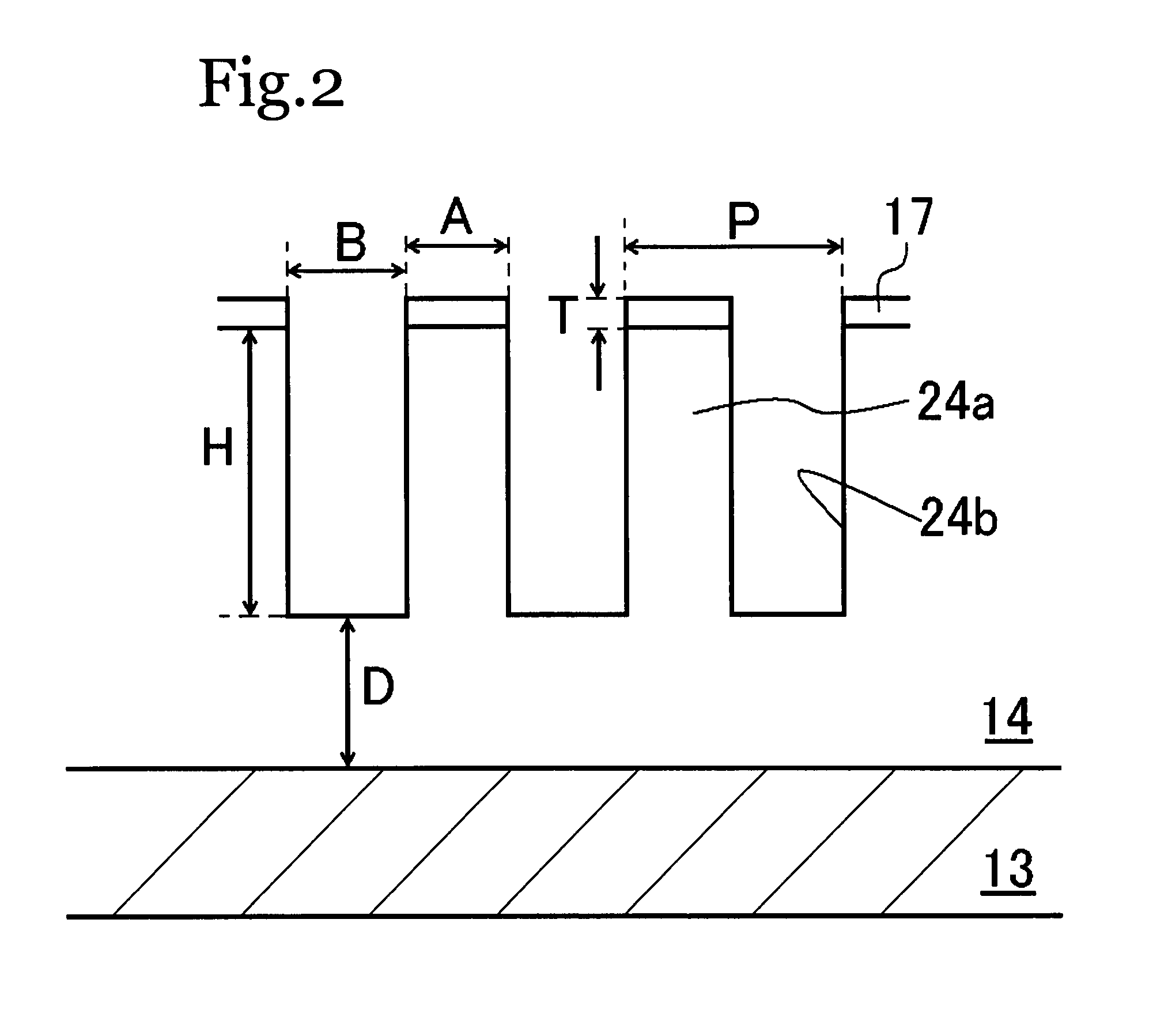
[0120]As shown in FIG. 4, the laser element in this Example is constituted the same as the laser element in Example 1, except that a region 18 with a high aluminum mixed crystal ratio, a thickness F of 5 nm, and a length E of 50 nm is formed on the side faces of the raised portions 24a of the diffraction grating 24 formed on a wave guide layer within a second semiconductor layer 14. The region 18 composed of AlGaN with a high aluminum mixed crystal ratio has the same aluminum content as the region 17 with a high aluminum mixed crystal ratio of the raised portions 24a, and the ratio thereof is 0.15.

[0121]This laser element is manufactured as follows.

[0122]After forming p-type wave guide layer, an SiO2 film (200 nm thick) is formed on this layer, and on this is formed a resist layer (200 nm thick). Using electron beam lithography, a pattern corresponding to diffraction grating is formed in the resist layer. This resist pattern is used as a mask to transfer the pattern to the SiO2 film...

example 3

[0126]As shown in FIG. 6, the laser element in this Example is constituted the same as the laser element in Example 1, except that the side faces of the recessed portions 24b the diffraction grating 24 formed on the wave guide layer in the second semiconductor layer 14 has a shape that is sloped at a slope angle γ of 60° or less and at a length G of 30 nm from the bottom face. Although not shown in FIG. 6, the region 17 with a high aluminum ratio is formed in a thickness of 35 nm on the top faces of the raised portions 24a in the shape shown in FIG. 8a.

[0127]This recessed and raised portions are manufactured as follows.

[0128]On the p-type wave guide layer, an SiO2 film (200 nm thick) is formed on this layer, and on this is formed a resist layer (200 nm thick). Using electron beam lithography, a pattern corresponding to diffraction grating is formed in the resist layer. This resist pattern is used as a mask to transfer the pattern to the SiO2 film, and then the SiO2 film and resist ...


PUM


Abstract

A nitride semiconductor laser element includes a substrate and a nitride semiconductor layer in which a first semiconductor layer, an active layer, and a second semiconductor layer are laminated in this order on the substrate. At least one of the first semiconductor layer and the second semiconductor layer includes a first section forming recessed and raised portions and a second section embedding the recessed and raised portions of the first section. A region with a higher aluminum mixed crystal ratio than the second section that embeds the recessed and raised portions is disposed on top faces of the raised portions. The nitride semiconductor layer defines resonant planes, and the recessed and raised portions are formed in a shape of stripes that extend substantially parallel to the resonant planes.

Description

CROSS-REFERENCE TO RELATED APPLICATIONS[0001]This application claims priority to Japanese Patent Application Nos. 2006-169221 and 2007-152772. The entire disclosure of Japanese Patent Application Nos. 2006-169221 and 2007-152772 are hereby incorporated herein by reference.BACKGROUND OF THE INVENTION[0002]1. Field of the Invention[0003]The present invention relates to a nitride semiconductor laser element, and more particularly relates to a nitride semiconductor laser element utilized a diffraction grating layer.[0004]2. Background Information[0005]Today it is considered possible to oscillate a semiconductor laser made from a nitride semiconductor over a wide range of wavelength bands, from the ultraviolet band to red, and such lasers can not only be used in DVDs and other such optical disk systems that allow information to be recorded and reproduced in large capacity and high density, but also hold promise as a light source or the like for laser printers, optical networks, and so on...

Claims


Application Information

Patent Timeline
Patent Type & Authority Patents(United States)
IPC IPC(8): H01L33/00H01S5/12
CPCB82Y20/00H01S5/12H01S5/0654H01S5/1231H01S5/2009H01S5/22H01S5/30H01S5/3063H01S5/34333H01S2301/173H01S2304/04H01S2304/12
Inventor MASUI, SHINGOTSUKAYAMA, KAZUTAKA
Owner NICHIA CORP
Why Eureka
Try Eureka