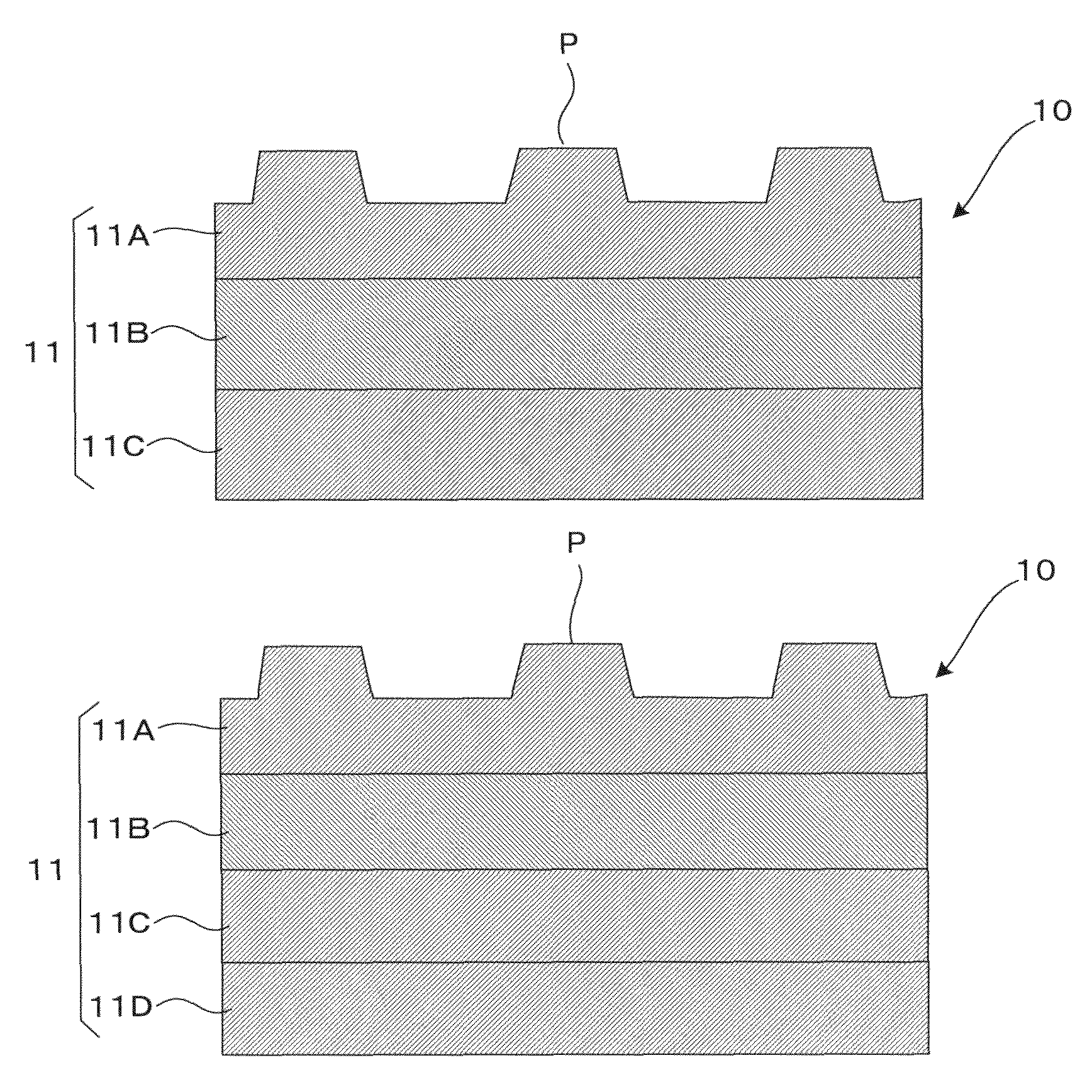
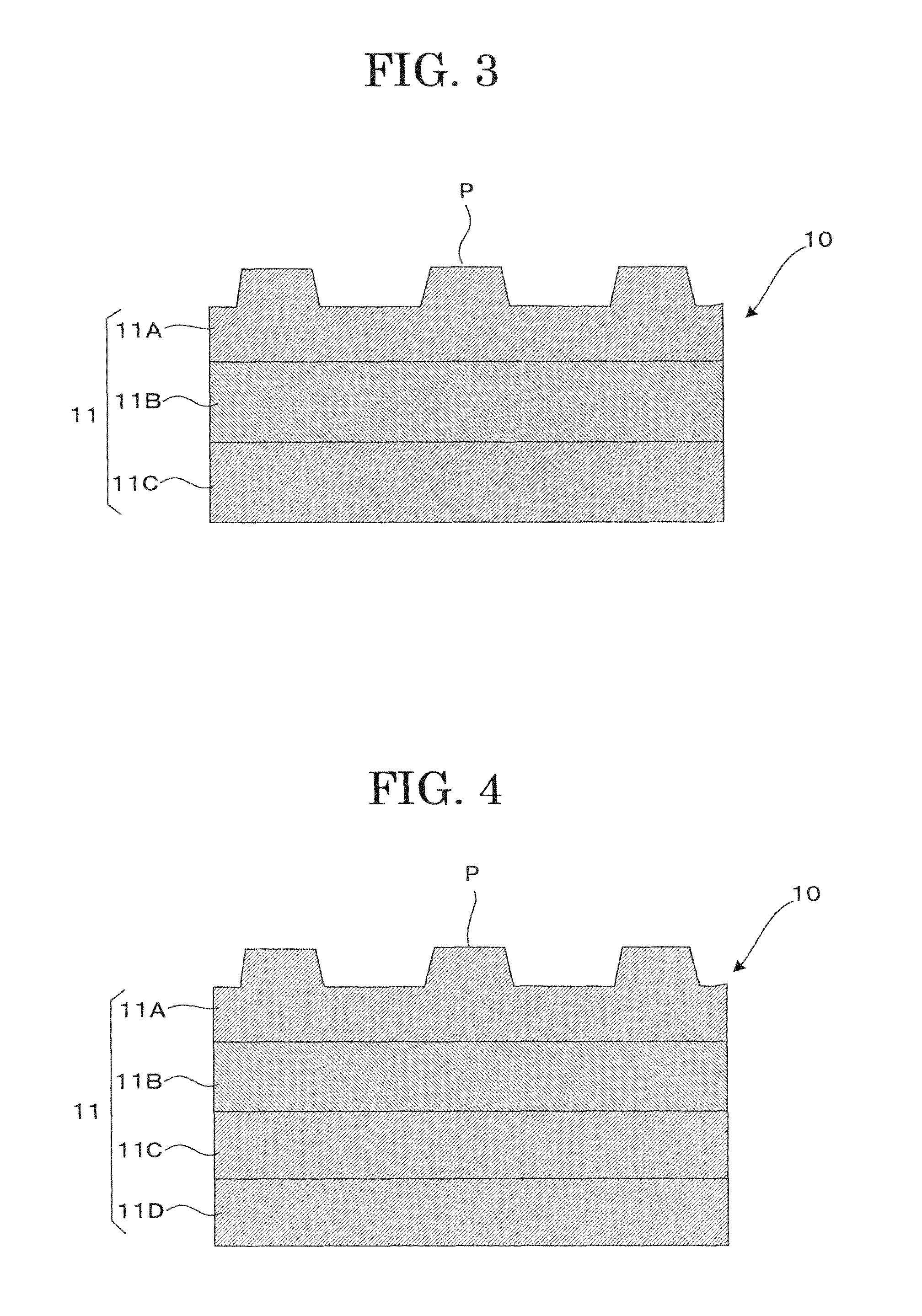
Mold, method for producing the same and magnetic recording medium
a technology of magnetic recording medium and mold, which is applied in the field of mold, can solve the problems of limited head processing, warpage or distortion of conventional stampers produced by the above-mentioned method, and the inability to increase the surface recording density of conventional improved methods, etc., and achieves the effect of superior flatness, small warpage amount, and small variation in the amount of warpag
- Summary
- Abstract
- Description
- Claims
- Application Information
AI Technical Summary
Benefits of technology
Problems solved by technology
Method used
Image

Examples
example 1
Production of Mold
[0120]As shown in FIG. 5A, on a substrate 15 made of a silicon wafer whose surface is flat, smooth and clean, a resist film 16 was formed by applying an electron beam resist solution by means of spin coating, etc. and baked. Then in an electron beam exposer (not shown in the figure) provided with a highly accurate rotational stage or X-Y stage, the substrate 15 mounted on the stage was irradiated with an electron beam B modulated correspondingly to a servo signal or the like, and a desired concavo-convex pattern P′ was created in the resist film 16 by means of drawing exposure.
[0121]Next, as shown in FIG. 5B, the resist film 16 underwent a developing process, and the desired concavo-convex pattern P′ was formed by the residual resist film 16 from which the exposed portion had been removed. A conductive layer (not shown in the figure) was provided on this concavo-convex pattern P′ by means of sputtering, and an original plate 17 which can be subjected to an electrof...
example 2
Production of Mold
[0143]A mold of Example 2 was produced in a similar manner to Example 1, except that the condition of the electroforming process in Example 1 was changed to such a condition that electroforming was conducted in three cycles at a current density of 6 A / dm2 for 70 min each.
[0144]The crystal orientation in cross section of the mold, the amount of warpage (the degree of flatness), and the variation in the amount of warpage were measured in a similar manner to Example 1, with respect to the mold of Example 2 obtained. The results are shown in Table 1.
[0145]As a result of an EBSD IPF image whereby the crystal orientation in cross section of the mold of Example 2 was measured, it was confirmed that first, second and third electroforming layers from the concavo-convex pattern side had the same crystal orientation in which Ni (110) was the preferred orientation.
example 3
Production of Mold
[0146]A mold of Example 3 was produced in a similar manner to Example 1, except that the condition of the electroforming process in Example 1 was changed to such a condition that after electroforming was conducted in two cycles at a current density of 6 A / dm2 for 95 min each, the current density was raised to 15 A / dm2 and sustained for 10 min.
[0147]The crystal orientation in cross section of the mold, the amount of warpage (the degree of flatness), and the variation in the amount of warpage were measured in a similar manner to Example 1, with respect to the mold of Example 3 obtained. The results are shown in Table 1.
[0148]As a result of an EBSD IPF image whereby the crystal orientation in cross section of the mold of Example 3 was measured, it was confirmed that first and second electroforming layers from the concavo-convex pattern side had the same crystal orientation in which Ni (110) was the preferred orientation, and that a third electroforming layer from the ...
PUM
| Property | Measurement | Unit |
|---|---|---|
| total thickness | aaaaa | aaaaa |
| thickness | aaaaa | aaaaa |
| size | aaaaa | aaaaa |
Abstract
Description
Claims
Application Information
 - R&D
- Intellectual Property
- Life Sciences
- Materials
- Tech Scout
- Unparalleled Data Quality
- Higher Quality Content
- 60% Fewer Hallucinations
Browse by: Latest US Patents, China's latest patents, Technical Efficacy Thesaurus, Application Domain, Technology Topic, Popular Technical Reports.
© 2025 PatSnap. All rights reserved.Legal|Privacy policy|Modern Slavery Act Transparency Statement|Sitemap|About US| Contact US: help@patsnap.com