Check patentability & draft patents in minutes with Patsnap Eureka AI!

Mold, method for producing the same and magnetic recording medium

a technology of magnetic recording medium and mold, which is applied in the field of mold, can solve the problems of limited head processing, warpage or distortion of conventional stampers produced by the above-mentioned method, and the inability to increase the surface recording density of conventional improved methods, etc., and achieves the effect of superior flatness, small warpage amount, and small variation in the amount of warpag

Inactive Publication Date: 2008-06-19
FUJIFILM CORP
View PDF3 Cites 8 Cited by
  • Summary
  • Abstract
  • Description
  • Claims
  • Application Information

AI Technical Summary

Benefits of technology

[0016]The object of the present invention is to provide a mold which is very small in the amount of warpage and superior in flatness, a method for producing a mold in which the variation in the amount of warpage is small and a highly accurate concavo-convex pattern can be efficiently formed, and a magnetic recording medium.
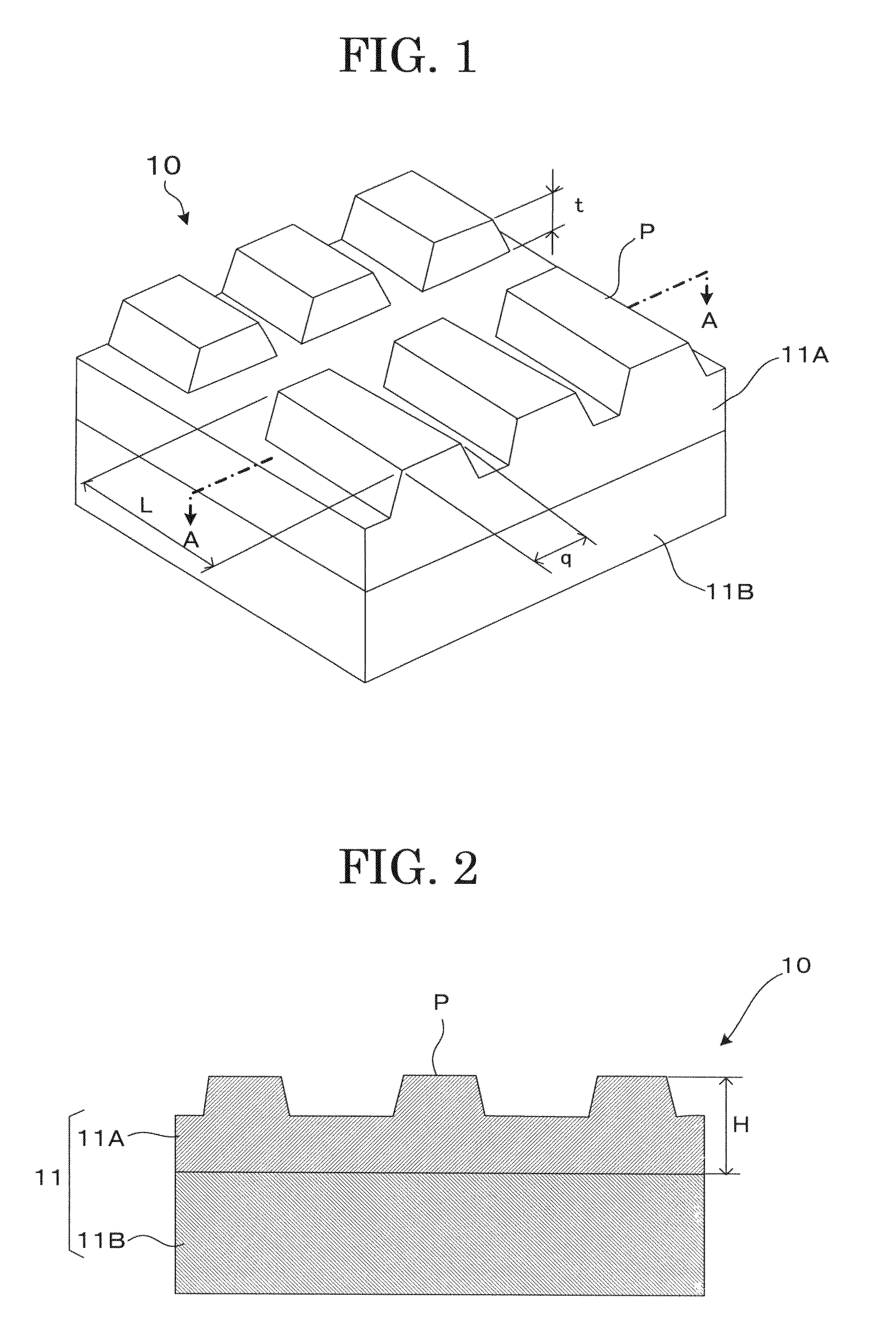
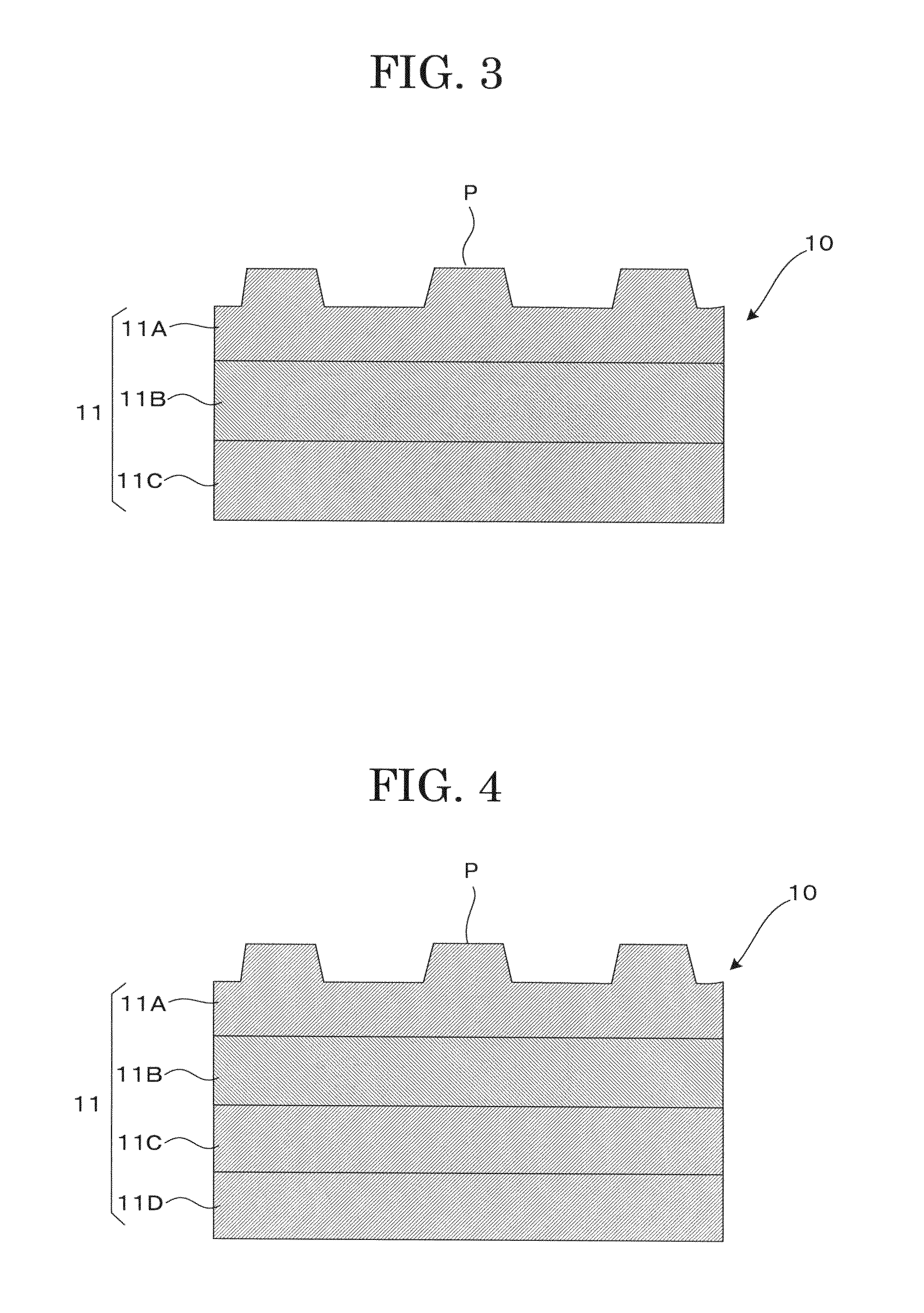
[0018]A mold of the present invention has a concavo-convex pattern on the surface thereof, and contains at least two electroforming layers, wherein the electroforming layers include at least two adjacent layers having the same crystal orientation. The mold of the present invention is able to prevent the formation of warpage as the mold has at least two electroforming layers having the same crystal orientation, the physical properties, and the stress distribution in the direction of the layer thickness contrary to the case where the electroforming layer is formed from a single layer. In addition, the mold of the present invention is able to prevent crystal grains from becoming coarse by laminating two or more electroforming layers. As a result, shear resistance of the mold when the layers are cut by punching becomes higher than in the case of a single-layer structure, the amount of warpage is therefore very small, and the flatness of the mold is greatly improved. The mold of the present invention can be suitably used for any of a stamper for a discrete track medium, a stamper for a patterned medium, or a master disk for magnetic transfer.
[0020]In the method for producing a mold of the present invention, by forming a mold of a metal plate containing two or more electroforming layers including at least two adjacent layers having the same crystal orientation, it is possible to efficiently produce the mold in which the electroforming layers are provided such that the variation in the amount of warpage is small and a highly accurate concavo-convex pattern can be formed.

Problems solved by technology

However, problems such as limitations of head processing, incorrect recording of information to another track situated next to a target recording track stemming from the widening of a magnetic field, and crosstalk at the time of reproduction have become conspicuous, and thus surface recording density can hardly be increased by conventional improved methods anymore.
However, conventional stampers produced by the above-mentioned method are not necessarily flat but often warped or distorted.
Hence, there is a problem that highly accurate concavo-convex patterns cannot be formed, as concavo-convex patterns formed are deformed or distorted.
However, conventional master disks produced by the above-mentioned method are not necessarily flat but often warped or distorted as a result of being deformed at the times of processes exemplified by the peeling step in which metal plates are peeled off original plates and the punching step in which the metal plates are cut by punching into predetermined sizes.
In addition, warpage and distortion may be caused by internal stress of electroforming layers in a photo-etching step as well.
When a master disk is warped or distorted as just described, there is a problem that it is impossible to improve the state in which the master disk and a slave disk are closely attached to each other and thus impossible to perform highly accurate magnetic transfer.
However, despite these attempts, the problems with adhesion have not completely been solved; in essence, it is necessary to improve the flatness of the master disk by removing the warpage or distortion of the master disk.
Also, there is a possibility that increasing adhesive pressure may damage or deform a concavo-convex pattern of the master disk, hence a cause of decrease in the durability of the master disk.

Method used


Image

  • Mold, method for producing the same and magnetic recording medium
  • Mold, method for producing the same and magnetic recording medium
  • Mold, method for producing the same and magnetic recording medium

Examples


example 1

Production of Mold

[0118]As shown in FIG. 5A, on a substrate 15 made of a silicon wafer whose surface is flat, smooth and clean, a resist film 16 was formed by applying an electron beam resist solution by means of spin coating, etc. and baked. Then in an electron beam exposer (not shown in the figure) provided with a highly accurate rotational stage or X-Y stage, the substrate 15 mounted on the stage was irradiated with an electron beam B modulated correspondingly to a servo signal or the like, and a desired concavo-convex pattern P′ was created in the resist film 16 by means of drawing exposure.

[0119]Next, as shown in FIG. 5B, the resist film 16 underwent a developing process, and the desired concavo-convex pattern P′ was formed by the residual resist film 16 from which the exposed portion had been removed. A conductive layer (not shown in the figure) was provided on this concavo-convex pattern P′ by means of sputtering, and an original plate 17 which can be subjected to an electrof...

example 2

Production of Mold

[0140]A mold of Example 2 was produced in a similar manner to Example 1, except that the condition of the electroforming process in Example 1 was changed to such a condition that electroforming was conducted in three cycles at a current density of 6 A / dm2 for 70 min each.

[0141]The crystal orientation in cross section of the mold, the amount of warpage (the degree of flatness), and the variation in the amount of warpage were measured in a similar manner to Example 1, with respect to the mold of Example 2 obtained. The results are shown in Table 1.

[0142]As a result of an EBSD IPF image whereby the crystal orientation in cross section of the mold of Example 2 was measured, it was confirmed that first, second and third electroforming layers from the concavo-convex pattern side had the same crystal orientation in which Ni (110) was the preferred orientation.

example 3

Production of Mold

[0143]A mold of Example 3 was produced in a similar manner to Example 1, except that the condition of the electroforming process in Example 1 was changed to such a condition that after electroforming was conducted in two cycles at a current density of 6 A / dm2 for 95 min each, the current density was raised to 15 A / dm2 and sustained for 10 min.

[0144]The crystal orientation in cross section of the mold, the amount of warpage (the degree of flatness), and the variation in the amount of warpage were measured in a similar manner to Example 1, with respect to the mold of Example 3 obtained. The results are shown in Table 1.

[0145]As a result of an EBSD IPF image whereby the crystal orientation in cross section of the mold of Example 3 was measured, it was confirmed that first and second electroforming layers from the concavo-convex pattern side had the same crystal orientation in which Ni (110) was the preferred orientation, and that a third electroforming layer from the ...


PUM

PropertyMeasurementUnit
total thicknessaaaaaaaaaa
thicknessaaaaaaaaaa
sizeaaaaaaaaaa

Abstract

There is provided a mold which contains at least two electroforming layers, wherein the mold has a concavo-convex pattern on a surface thereof, and the electroforming layers include at least two adjacent layers having the same crystal orientation.

Description

BACKGROUND OF THE INVENTION[0001]1. Field of the Invention[0002]The present invention relates to a mold suitable for a stamper for a discrete track medium, a stamper for a patterned medium, a master disk for magnetic transfer, and the like; a method for producing the mold; and a magnetic recording medium.[0003]2. Description of the Related Art[0004]In recent years, for magnetic recording media, remarkable increase in surface recording density has been achieved by means of improvements such as reduction in the size of magnetic particles constituting recording layers thereof, alteration of materials and minuteness in head processing, and, for the future too, further increase in surface recording density is hoped for.[0005]However, problems such as limitations of head processing, incorrect recording of information to another track situated next to a target recording track stemming from the widening of a magnetic field, and crosstalk at the time of reproduction have become conspicuous, ...

Claims


Application Information

Patent Timeline
Patent Type & Authority Applications(United States)
IPC IPC(8): B29C59/00B29C33/56B29C33/42C25D1/10B81C99/00
CPCB29L2017/005B82Y10/00C25D1/10C25D5/10G11B11/10582G11B5/855G11B5/865G11B7/261G11B7/263G11B5/743C25D5/617
Inventor ICHIKAWA, KENJIKASAHARA, SEIJI
Owner FUJIFILM CORP
Features
  • R&D
  • Intellectual Property
  • Life Sciences
  • Materials
  • Tech Scout
  • Unparalleled Data Quality
  • Higher Quality Content
  • 60% Fewer Hallucinations
Learn More