However, by using the die-to-
database comparison method for
wafer inspection, corner roundness of a pattern formed on a
wafer is likely to be detected as a defect.
However, in the inspection of a wafer, because the corner roundness added by the pretreatment may be different from corner roundness of each pattern actually formed on the wafer, the pretreatment may not perfectly prevent the corner roundness of the pattern from being detected as the defect.
As a result, a problem in which a fine defect existing in a place except a corner cannot be detected has happened.
However, the above problem is severe for the die-to-
database comparison wafer inspection, because a pattern formed on the wafer is allowed to be deformed as long as an electrical property is guaranteed.
Therefore, the die-to-
database comparison wafer inspection has not been put into practical use.
Because the repeated defects occur in a die to-be-inspected and in adjacent dies that are to be compared with the die to-be-inspected, the die-to-die comparison wafer inspection cannot detect the repeated defects.
Although the die-to-die comparison wafer inspection has not been put into practical use because of calculation cost or the like, there have been proposed inspection methods in which
design data and a wafer image are used.
However, these methods fail to realize an inspection speed that is
usable in high-speed inspection, and fail to perform matching while detecting a pattern deformation quantity.
However, the method cannot classify whether the defect is a killer defect or not, because the method cannot recognize which part of a circuit the defect destroys.
Moreover, a position of a defect detected by the die-to-die comparison inspection has an error caused by precision of a stage and an optical
system of an inspection apparatus, and such error is approximately ten or more times larger than a
line width of a pattern to-be-inspected.
Due to the error, even if a defect position is related with design data, relationship between the defect position and the design data cannot be recognized.
If the OPC pattern does not effectively correct a pattern formed on a wafer, repeated defects occur.
However, the die-to-die comparison wafer inspection cannot detect the repeated defects.
In addition, in a multi-product / small-volume fabricating process, e.g. a
system-on-a-
chip (SoC) fabricating process, a short delivery time is required.
In the fabricating process, when repeated defects are detected in electric inspection as a final inspection, a short delivery time cannot be achieved.
Although the entire device can be verified by the
lithography simulator, the
simulation pattern cannot be necessarily the same as an actual pattern.
Moreover, a defect except for a defect caused by the OPC pattern cannot be detected by the
lithography simulator.
However, currently, the control of the two-dimensional shape is performed by a human work, and is not perfectly performed.
1. In order to detect repeated defects in each
semiconductor device, it is practically difficult to check whether there are defects at the same location by checking huge defect information.
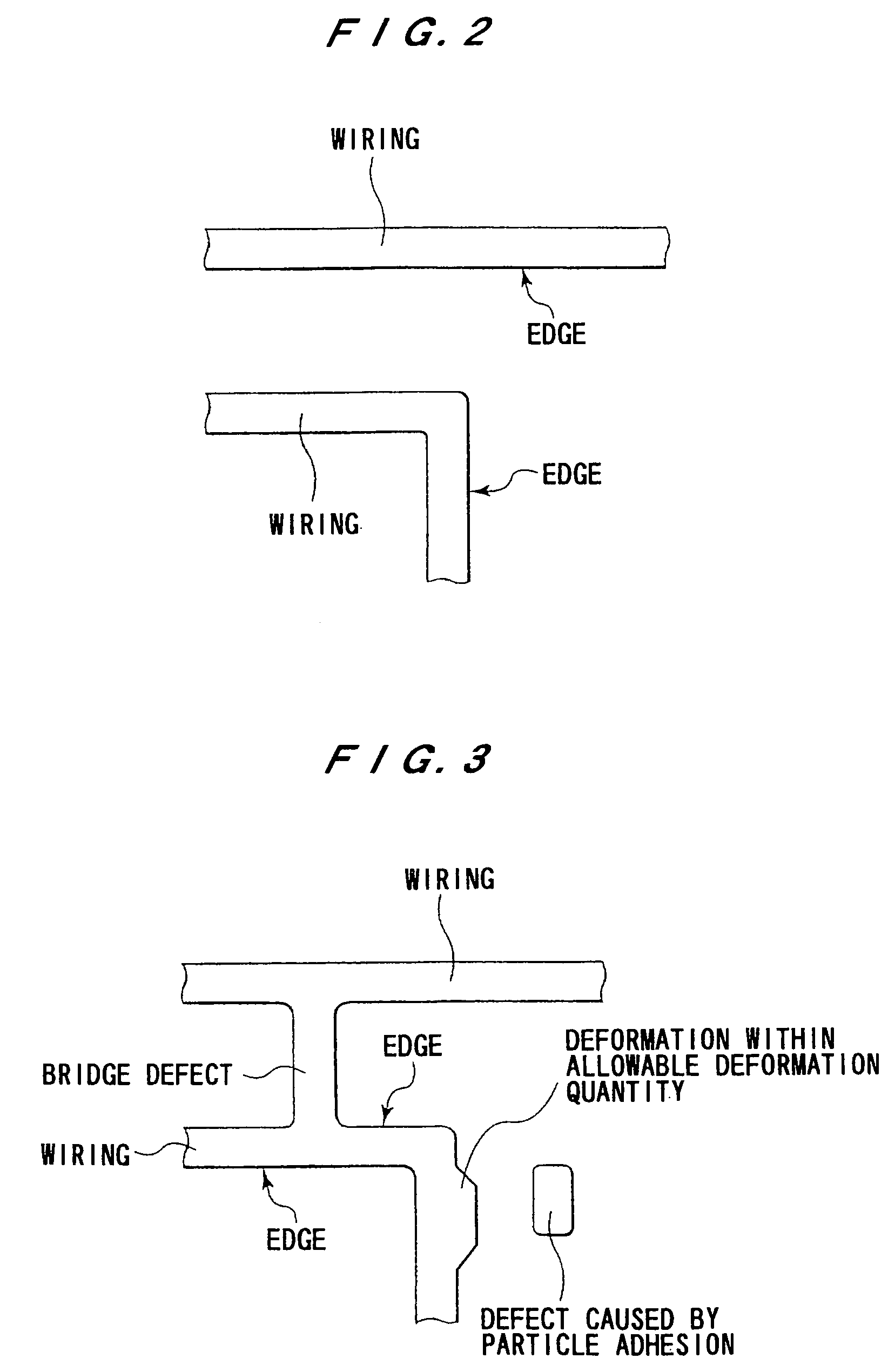
2. An end except for an end-cap and an end of a wiring pattern to be connected to a
contact hole / via hole may not be corrected by an OPC pattern correctly. Even if the end is shrunken by more than an allowable pattern deformation quantity for an end-cap or an end of a wiring pattern to be connected to a
contact hole / via hole, it is not necessary to recognize the shrunken end as a defect.
3. Conventionally, an
overlay error is controlled by measuring limited areas in a
semiconductor device. Therefore, the
overlay error caused locally by a
stepper aberration or the like cannot be controlled.
4. The conventional die-to-die comparison method is performed by comparing corresponding two images. In this method, because the corresponding two images to be compared have different relationship between a pattern to-be-inspected and pixel boundaries, it is necessary for luminance values of pixels to be interpolated so that the two images have the same relationship between the pattern to-be-inspected and the pixel boundaries. A problem in which inspection accuracy becomes low by the interpolation arises.
5. A contour obtained from the second edges can be used for input data of a
lithography simulator or the like. In this case, it is necessary to input the contour indirectly, because lithography simulator
processing is slower than contour output
processing.
6. The optimal allowable pattern deformation quantity depends on a desirable electrical property. Therefore, it is necessary to provide a method of obtaining an optimal allowable pattern deformation quantity by inspecting a standard specimen, which is judged as a
semiconductor device having good quality.
7. For improving quality of semiconductor device, it is necessary for all gate widths in a semiconductor device to be measured, the measured gate widths are classified based on gate lengths, the minimum distances to the nearest pattern, or the like, and the gate widths are analyzed. However, by using a conventional CD-SEM, only a limited number of gate widths in a semiconductor device can be measured and classified practically.
8. As a method of improving quality of an image of a pattern to-be-inspected, the image-accumulation method is well known. However, in the case where images of a pattern to-be-inspected on a specimen liable to cause the
electrification phenomenon are acquired successively, a sharp accumulated image cannot be obtained by accumulating the acquired images simply, because the acquired images are distorted gradually.
9. In the case of large
distortion quantities of the image of the pattern to-be-inspected, vectors between a reference pattern and edges of an image of a pattern to-be-inspected that exceed an allowable deformation quantity cannot be obtained, and therefore the
distortion quantities of the image of the pattern to-be-inspected may not necessarily be obtained accurately.
However, by using the method, an image of a pattern to-be-inspected cannot be acquired by performing interlace scan or image-accumulation scan.
In addition, because a large area is scanned repeatedly, a specimen is drastically damaged by an
electron beam scanning.
However, a tendency for pattern deformation quantities with regard to line widths of line parts of patterns to-be-inspected, and a tendency for pattern deformation quantities with regard to space widths of the line parts or a tendency for edge placement errors of ends of the patterns to-be-inspected may be different.
In such case, if a
process window is obtained from the results of measurement with regard to the line widths of the line parts of the patterns to-be-inspected, a semiconductor fabricated by
exposure under conditions in the
process window may have a defect.
However, there has not been a method in which the
shaped beam, which is deformed during the
exposure of the
photomask pattern of the product, is controlled.

