Methods for controlling dopant concentration and activation in semiconductor structures

a technology of dopant concentration and activation, which is applied in the direction of semiconductor devices, electrical equipment, basic electric elements, etc., can solve the problems of increasing physical dimensions, affecting the feature size and spacing requirements of electrical components in dense integrated electrical circuits, and not having known manufacturing solutions to meet the requirements of rapidly evolving devices

Inactive Publication Date: 2010-12-07
THE BOARD OF TRUSTEES OF THE UNIV OF ILLINOIS
View PDF28 Cites 102 Cited by
  • Summary
  • Abstract
  • Description
  • Claims
  • Application Information

AI Technical Summary

Benefits of technology

[0014]The present invention provides methods for fabricating semiconductor structures and devices, particularly ultra-shallow doped semiconductor structures exhibiting low electrical resistance. Methods of the present invention allow fabrication of a doped semiconductor structure having a selected dopant concentration depth profile, which provides useful junctions and other device components in microelectronic and nanoelectronic devices, such as transistors in high density integrated circuits. It is an object of the present invention to provide methods and devices for electrically activating semiconductor dopants that exhibit low dopant losses and reduced dopant diffusion with respect to conventional thermal processing methods. It is another object of the present invention to provide methods for precisely controlling dopant diffusion in lateral and vertical dimensions during thermal processing. It is further an object of the present invention to provide improved ion implantation and annealing methods that are compatible with existing semiconductor processing and device fabrication techniques and, thus, are easily integrated into well developed semiconductor technologies.
[0015]In one aspect, the present invention provides a method for making a doped semiconductor wherein the rate and / or extent of dopant diffusion during annealing is selectively adjustable. In an embodiment, a semiconductor having an exposed surface is provided and the exposed surface is treated with a surface modifying agent. Interaction between the surface modifying agent and the semiconductor forms diffusion control groups on the exposed surface. Preferably for methods providing selected semiconductor dopant concentrations and concentration depth profiles, a selected surface abundance of the diffusion control groups are generated on the exposed surface of the semiconductor. Dopant is implanted into the semiconductor, and the semiconductor having implanted dopant is annealed, thereby generating a semiconductor having electrically activated dopant. In this embodiment of the present invention, selection of the surface abundance of diffusion control groups controls the rate and / or extent of diffusion of dopant during annealing by adjusting the rates of important diffusion-related processes that couple the surface and bulk phases of a semiconductor structure. Selection of the surface abundance of diffusion control groups in methods of the present invention also controls the rate of dopant loss to the surface during annealing and may be used to provide efficient dopant activation with low dopant loss.

Problems solved by technology

The International Technology Roadmap for Semiconductors currently acknowledges, however, that there are no known manufacturing solutions to satisfy these rapidly evolving device requirements.
Accordingly, fabrication of extremely shallow dopant-containing semiconductor layers having low electrical resistance, such as dopant-containing layers comprising P-N junctions in CMOS transistors, is a fundamental barrier to continued advances in the performance of many microelectronic devices.
Furthermore, thermal diffusion methods are susceptible to problems associated with lateral diffusion of dopants, poor control of dopant concentrations and a propensity to generate dislocations, which can significantly impede satisfaction of the feature size and spacing requirements of electrical components in dense integrated electrical circuits.
Subsequent annealing of the dopant-containing layer, however, inevitably causes dopant atoms to diffuse, thereby increasing the physical dimensions of the dopant-containing layer.
Current annealing technologies have run into a limit in their ability to simultaneously increase dopant activation and decrease dopant diffusion, especially for the key dopant boron.
This problem has been worsened by the need to continually reduce processing temperatures to avoid damaging structures already in place during device fabrication.
These complex diffusion mechanisms constitute a fundamental limit on the control of physical dimensions of dopant-containing layers prepared by ion implantation methods and currently impede reproducible fabrication of ultra-shallow (<200 nm) dopant-containing layers.
The undesirable effects of TED are exacerbated by the higher concentrations of active dopant required for improved microelectronic device performance.
Such high concentrations are well above the thermodynamic solubility limit and, thus the corresponding structures are thermodynamically unstable.
Ion implantation at the high ion fluxes required to achieve such dopant concentrations creates a large number of defects and interstitials in the bulk phase of the semiconductor substrate which promotes fast TED of the dopants during annealing.
These TED mechanisms involving interstitials ultimately results in significant junction deepening.
In addition, implantation at high ion fluxes may generate electrically charged defect sites residing at the exposed surface of the semiconductor layer in sufficient numbers that they couple to the motion of charge defects in the underlying bulk.
Such defect engineering methods, however, have generally demonstrated limited utility.
While these methods may effectively limit the occurrence of TED, implementation of these methods is expected to require solutions to a large number of problems associated with integration of these methods into existing and well developed semiconductor processing techniques.
Such integration issues remain a significant barrier to adoption of these approaches for fabricating ultra-shallow dopant-containing semiconductor layers.
The methods provided are limited, however, to techniques wherein the nitrogen provided to the semiconductor substrate is implanted to depths in the bulk phase of the semiconductor roughly equivalent to the implanted dopant, and the application indicates that implantation of nitrogen into the bulk unavoidably introduces damage to the semiconductor substrate.
Further, although the application asserts that TED can be reduced, it is unclear if the disclosed methods also provide a means of increasing electrical activation of implanted dopant materials.
Although the application indicates that TED in the thin semiconductor layer can be reduced, it is unclear if the disclosed methods also provide a means of increasing the electrical activation of implanted dopant materials.
As device dimensions scale downward, however, the procedures disclosed in Downey et al. provide insufficient flexibility for optimally adjusting the loss rates of silicon interstitials and / or dopants.
For example, too little O2 results in disappearance of the oxide surface layer leading to loss of too much dopant, and too much O2 injects unwanted silicon interstitials into the bulk yielding oxygen-enhanced diffusion.

Method used


Image

  • Methods for controlling dopant concentration and activation in semiconductor structures
  • Methods for controlling dopant concentration and activation in semiconductor structures
  • Methods for controlling dopant concentration and activation in semiconductor structures

Examples


example 1

Numerical Simulations and Experimental Observations of Dopant Diffusion and Activation Control Provided by Selective Variation of Surface Loss Probability for Interstitial

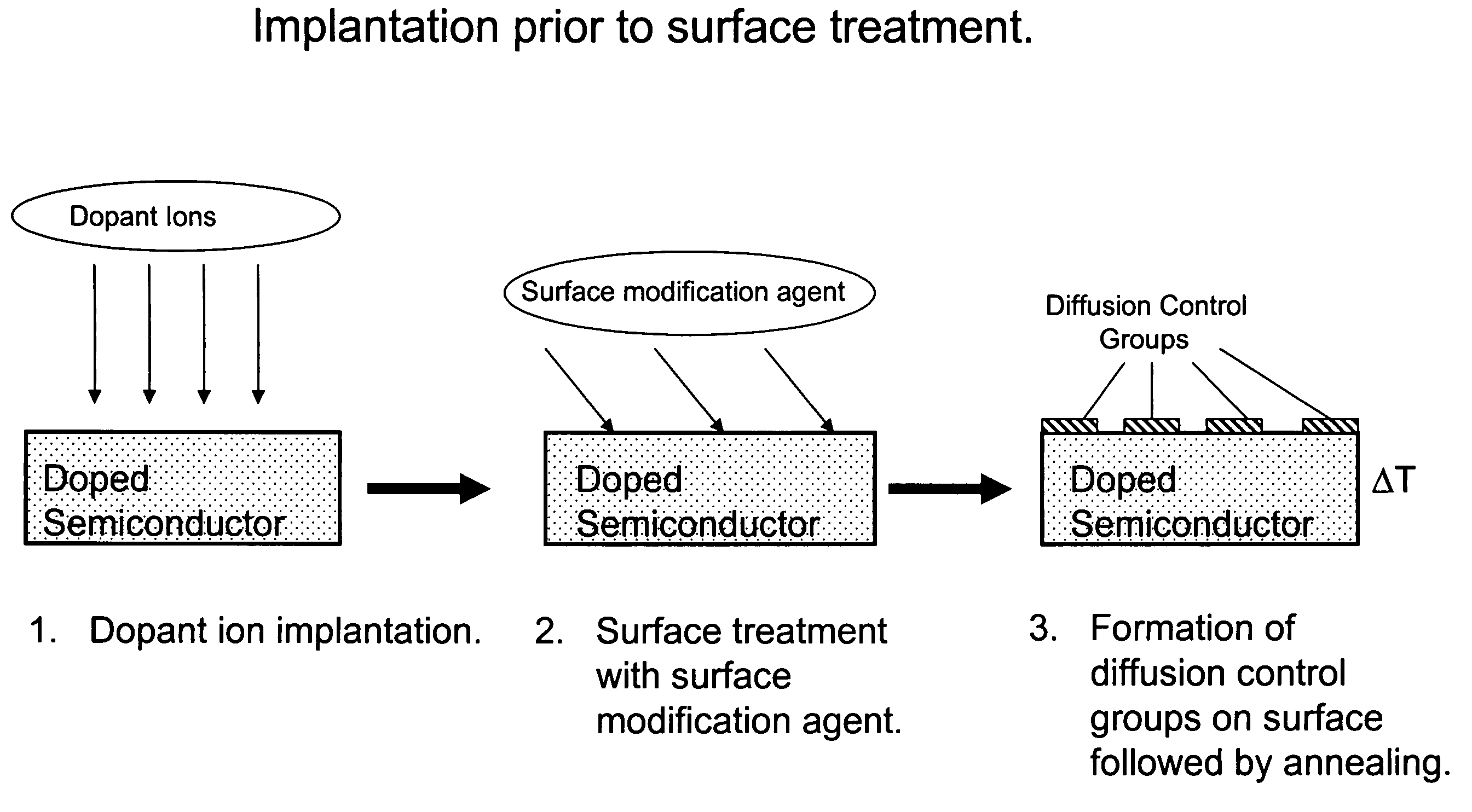
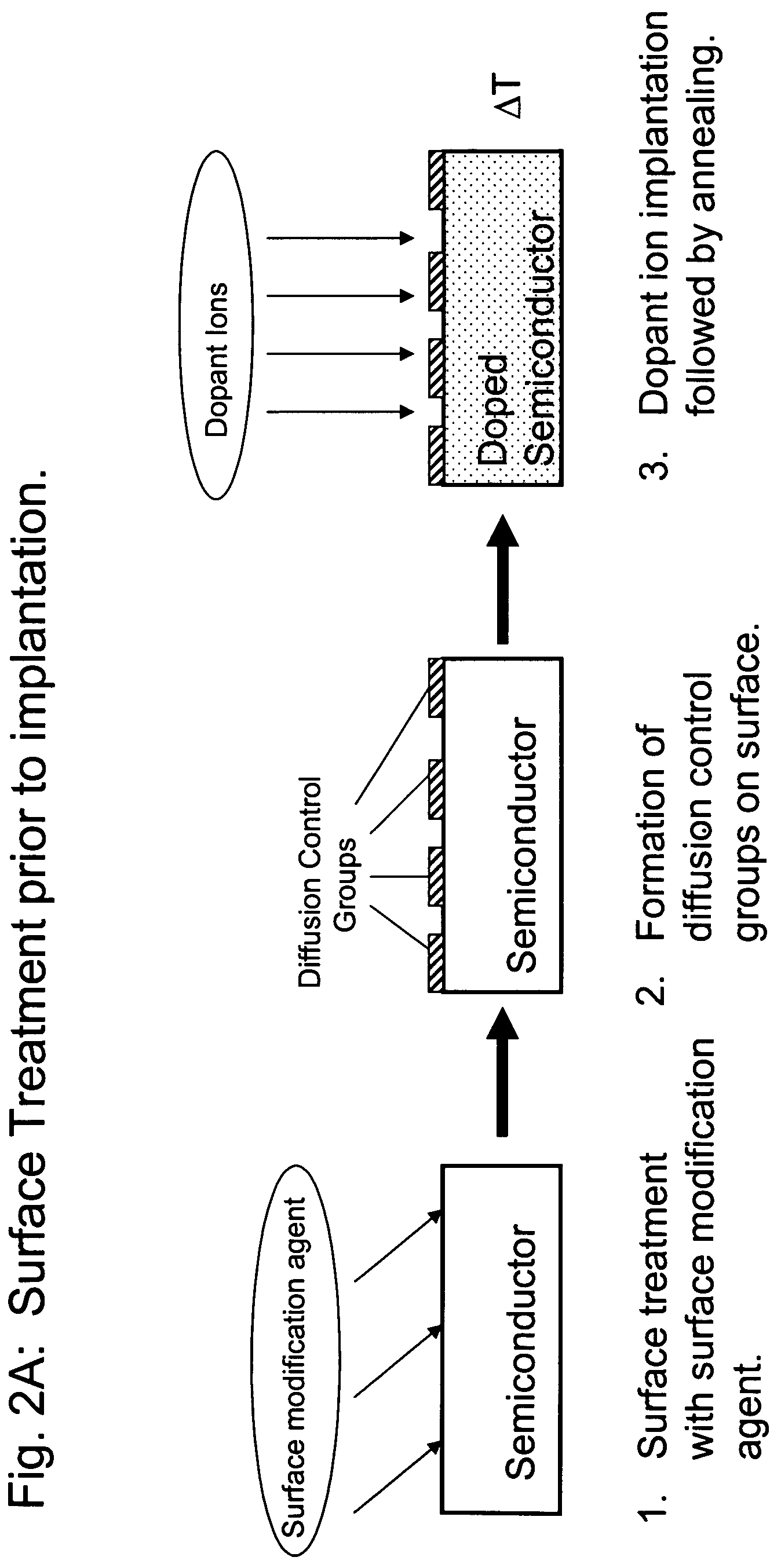
[0085]The ability of the present methods to control dopant diffusion and electrical activation was verified by numerical simulations. Specifically, it is a goal of the present invention to provide methods of making doped semiconductor structures having a selected dopant concentration depth profile. Further, it is a goal of the present invention to provide methods of making ultra-shallow doped semiconductor structures that exhibit low dopant loss and having low electrical resistance.

1. Computational Approach:

[0086]To model bulk-surface coupling in semiconductor dopant diffusion, we have developed a computational model for diffusion and dopant activation, primarily for simulating boron implanted in silicon, by adapting the simulator FLOOPS 2000 (by Mark E. Law of the University of Florida and Al Tasch of the Universi...

example 2

The Use of Nitrogen Release Gases as Surface Modification Agents in the Methods of the Present Invention

[0107]Gases that release nitrogen to semiconductor surfaces, such as ammonia or hydrazine, comprise particularly useful surface modification agents in the methods of the present invention. Exposure of a semiconductor surface to surface modifying groups that release nitrogen, under some conditions, forms nitride (Si3N4) on the treated surface. This mechanism of surface treatment avoids two major problems that plague surface manipulation using surface modification agents comprising oxygen. First, silicon-nitrogen compounds do not readily volatilize from the Si surface. Second, nitride growth injects vacancies instead of interstitials into the underlying Si. The lack of volatilization removes an important constraint in controlling surface-bulk coupling, since in principle no nitrogen-containing gas would need to be added during heating for nitride replenishment. And if such a gas wer...

example 3

Controlling Defect Concentrations in Bulk Semiconductor Materials Via Surface Adsorption

[0110]In addition to providing a means of controlling diffusion and activation of dopants implanted in semiconductor materials, the methods of the present invention also provide a means of controlling the concentrations and concentration depth profiles of defects in bulk semiconductors. Specific modification of the surfaces of undersaturated semiconductor materials, such as heated unimplanted semiconductors, by treatment with surface modifying agents provides a means of selectively controlling the concentrations and concentration depth profiles of vacancies and interstitials in bulk semiconductors. In such undersaturated semiconductor materials, dangling, free bonds at the surface act as sources of defects by releasing interstitials into the bulk under some conditions. The strength of this source of interstitials is selectable in the present invention by modifying the composition of the surface, ...


PUM


Abstract

The present invention provides methods for fabricating semiconductor structures and devices, particularly ultra-shallow doped semiconductor structures exhibiting low electrical resistance. Methods of the present invention use modification of the composition of semiconductor surfaces to allow fabrication of a doped semiconductor structure having a selected dopant concentration depth profile, which provides useful junctions and other device components in microelectronic and nanoelectronic devices, such as transistors in high density integrated circuits. Surface modification in the present invention also allows for control of the concentration and depth profile of defects, such as interstitials and vacancies, in undersaturated semiconductor materials.

Description

CROSS-REFERENCE TO RELATED APPLICATIONS[0001]This application claims priority under 35 U.S.C. 119(e) to U.S. provisional Patent Application 60 / 592,902 filed Jul. 30, 2004, which is hereby incorporated by reference in its entirety to the extent not inconsistent with the disclosure herein.STATEMENT REGARDING FEDERALLY SPONSORED RESEARCH OR DEVELOPMENT[0002]This invention was made, at least in part, with United States governmental support awarded by National Science Foundation Grants CTS 98-06329 and 02-03237. The United States Government has certain rights in this invention.BACKGROUND OF INVENTION[0003]The continuing trend toward smaller, higher speed microelectronic devices requires integrated circuit designs characterized by smaller feature sizes and closer spacing between electrical components. These requirements have generated an immediate demand for methods for fabricating extremely shallow and spatially well defined dopant-containing semiconductor layers that exhibit very low el...

Claims


Application Information

Patent Timeline
Patent Type & Authority Patents(United States)
IPC IPC(8): H01L21/38
CPCH01L21/306H01L21/26513H01L21/324Y10S438/914Y10S438/92H01L21/2658H01L21/26566
Inventor SEEBAUER, EDMUND G.BRAATZ, RICHARD D.JUNG, MICHAEL YOO LIMGUNAWAN, RUDIYANTO
Owner THE BOARD OF TRUSTEES OF THE UNIV OF ILLINOIS
Why Eureka
Try Eureka