

Method of manufacturing a semiconductor device including a semiconductor substrate with stripes of different crystal plane directions
a manufacturing method and technology of semiconductor devices, applied in the direction of semiconductor devices, basic electric elements, electrical appliances, etc., can solve the problems of difficult to increase the operation characteristics of the circuit, and achieve the effect of improving the field effect mobility of each tft, low voltage driving, and high operating characteristics
- Summary
- Abstract
- Description
- Claims
- Application Information
AI Technical Summary
Benefits of technology
Problems solved by technology
Method used
Image

Examples
embodiment mode 1
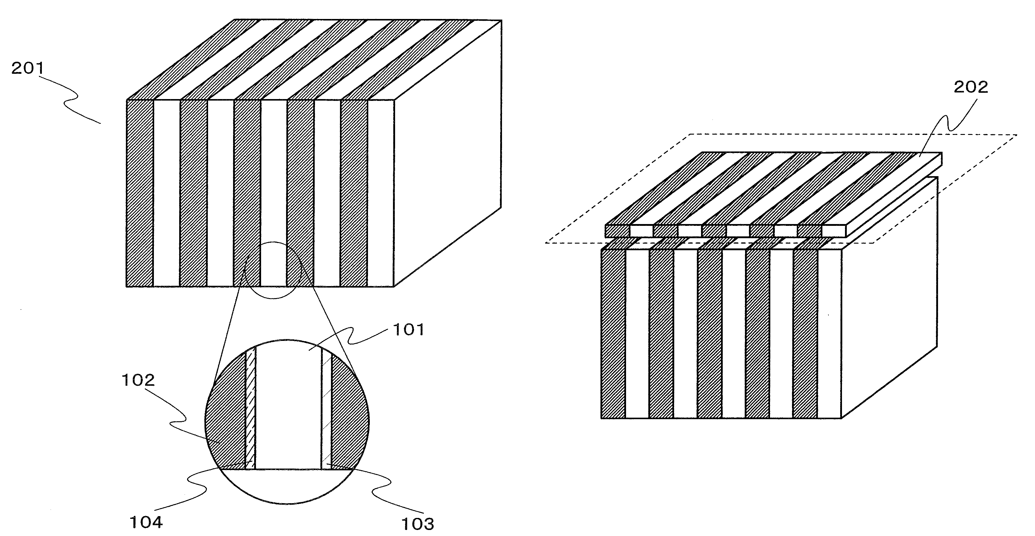
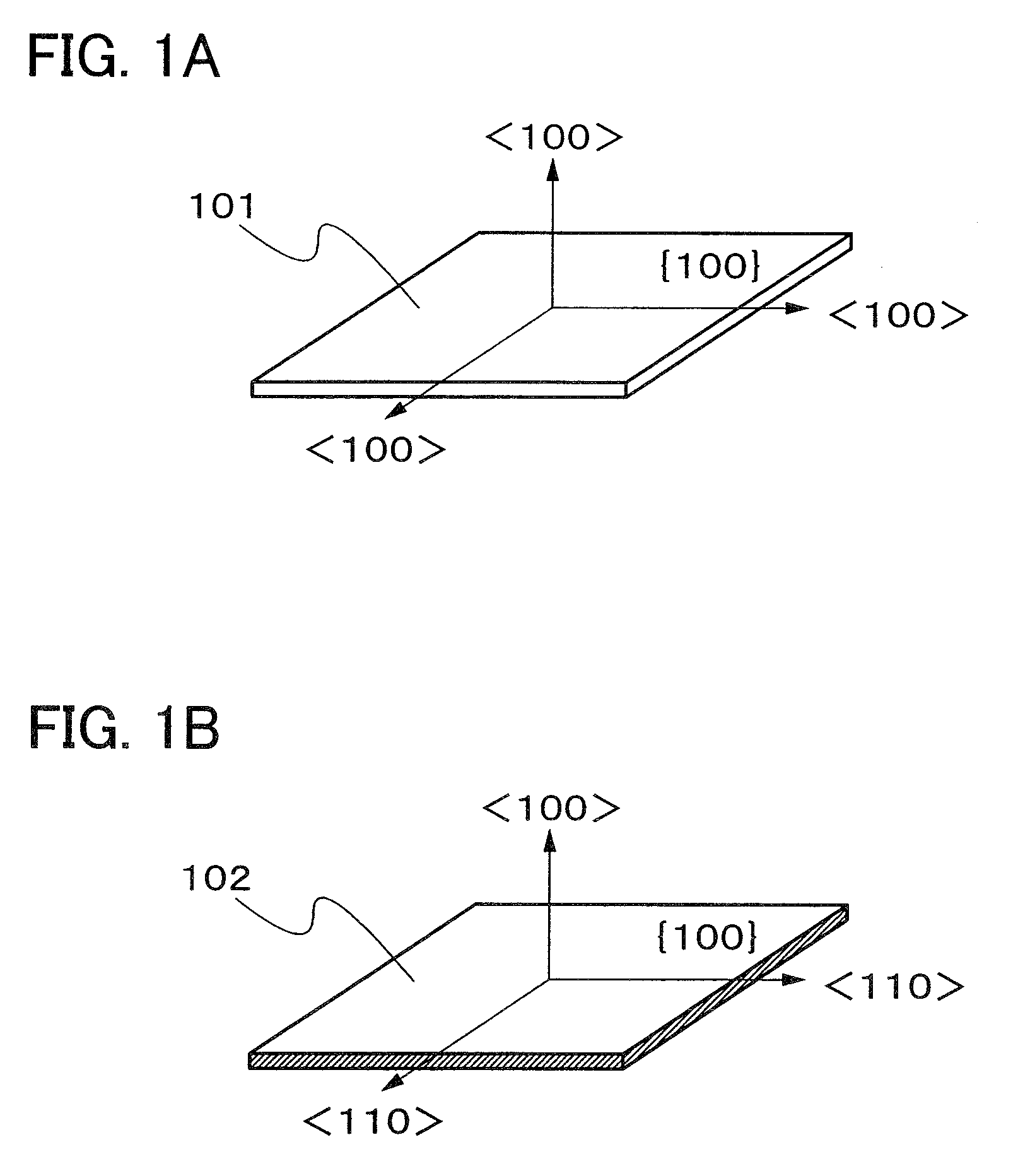
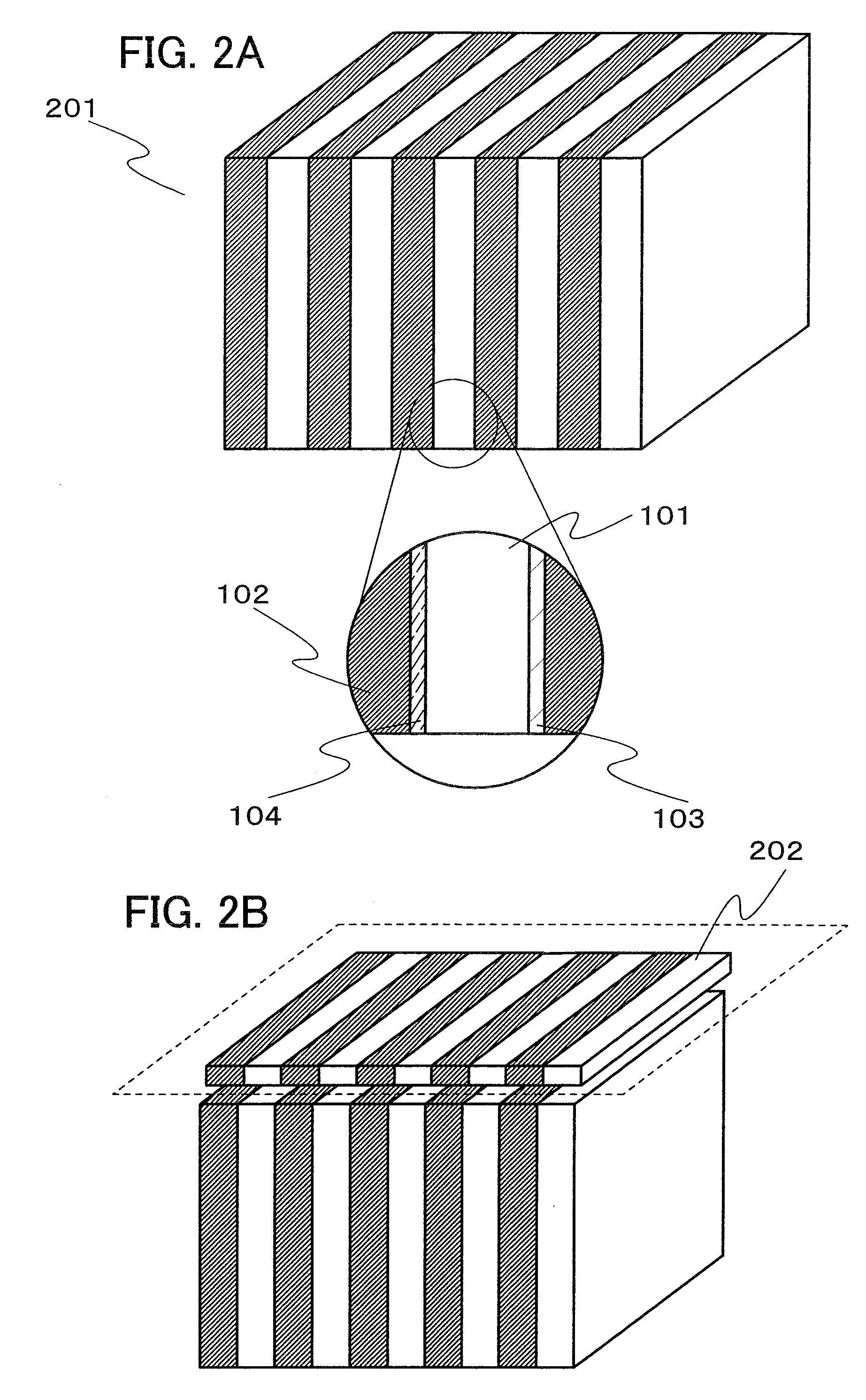
[0034]In this embodiment mode, a process for forming a single crystal semiconductor layer having different crystal plane directions over an insulating substrate will be described. First, a semiconductor substrate having n-type conductivity whose crystal plane direction is {100} is processed to have a quadrangular shape. At this time, a first semiconductor substrate 101 is formed so that the crystal plane direction of a side surface of the substrate is {100} (see FIG. 1A). In a similar manner, a semiconductor substrate having p-type conductivity whose crystal plane direction is {100} is processed to have a quadrangular shape. At this time, a second semiconductor substrate 102 is formed so that the crystal plane direction of a side surface of the substrate is {110} (see FIG. 1B). In this embodiment mode, a semiconductor substrate of silicon, gallium arsenide, indium phosphide, or the like can be used for the first semiconductor substrate 101 and the second semiconductor substrate 102....
embodiment mode 2
[0050]Although a semiconductor substrate whose crystal plane direction is {100} is used in Embodiment Mode 1, the case where a semiconductor substrate 212 is manufactured using a semiconductor substrate whose crystal plane direction is {110} will be described in this embodiment mode as shown in FIGS. 5A, 5B, 6A, and 6B
[0051]First, a semiconductor substrate having p-type conductivity whose crystal plane direction is {110} is processed to have a quadrangular shape. At this time, a first semiconductor substrate 111 is formed so that alternate arrangement of crystal plane directions {100} and {110} appears on a side surface of the substrate (see FIG. 5A). In a similar manner, a semiconductor substrate having n-type conductivity whose crystal plane direction is {110} is processed to have a quadrangular shape. At this time, a second semiconductor substrate 112 is formed so that alternate arrangement of crystal plane directions {100} and {110} appears on a side surface of the substrate (se...
embodiment mode 3
[0057]In this embodiment mode, an example of a process for manufacturing an inverter circuit which is one example of a semiconductor device using a CMOS circuit will be described. Note that the present invention is not limited to such a simple circuit and can realize various integrated circuits such as a microprocessor. FIGS. 7A, 8A, 9A, 10A, 11A, 12A, and 13A each are a top view of an inverter circuit, and FIGS. 7B, 8B, 9B, 10B, 11B, 12B, and 13B each are a cross sectional view taken along A-B in each of FIGS. 7A, 8A, 9A, 10A, 11A, 12A, and 13A.
[0058]A semiconductor device formed using an SOI substrate which is formed in such a manner that a semiconductor layer 306 shown in FIG. 4 is formed over an insulating substrate 305 with an insulating film 417 interposed therebetween is manufactured. A quadrangular semiconductor substrate 212 shown in FIG. 6B of the Embodiment 2 may be used to form the semiconductor layer. First, the semiconductor layer 306 is etched to have an island shape,...
PUM
 Abstract
Description
Claims
Application Information