Method for manufacturing SOI wafer and SOI wafer

a manufacturing method and technology for soi wafers, applied in semiconductor/solid-state device manufacturing, basic electric elements, electric devices, etc., can solve the problems of complicated process or cost increase, limit the uniformity of soi layer film thickness, and increase the cost of manufacturing, so as to achieve efficient manufacturing and less slip dislocation

Active Publication Date: 2011-02-22
SHIN-ETSU HANDOTAI CO LTD
View PDF11 Cites 4 Cited by
  • Summary
  • Abstract
  • Description
  • Claims
  • Application Information

AI Technical Summary

Benefits of technology

Therefore, in view of the above-explained problems, it is an object of the present invention to provide a method for manufacturing an SOI wafer that is a method for manufacturing a high-quality SOI wafer with less slip dislocation and others in which a thickness of an SOI layer is increased by growing an epitaxial layer on the SOI layer of the SOI wafer having an oxide film and the SOI layer formed on a base wafer.
In the method for manufacturing an SOI wafer in which a thickness of the SOI layer is increased by growing the epitaxial layer on the SOI layer of the SOI wafer having the oxide film and the SOI layer formed on the base wafer, since setting the reflectivity on the surface of the SOI wafer for the heating lamp light to the range of 30% to 80% enables efficiently performing absorption of an energy of the heating lamp light on the surface of the SOI wafer, a temperature distribution in the SOI wafer can be further uniformed, and occurrence of slip dislocation and others can be suppressed. Therefore, the high-quality SOI wafer with less slip dislocation and others can be efficiently obtained, thereby improving productivity.
The reflectivity on the surface of the SOI wafer having the SOI layer with a small film thickness may be greatly contributed by formation of a one-dimensional photonic bandgap structure including the oxide film and the SOI layer in some cases. Thus, respectively adjusting the thicknesses of the oxide film and the SOI layer of the SOI wafer on which the epitaxial layer is grown enables setting the reflectivity of the surface of the SOI wafer to fall within the range of 30% to 80%.
An effect of the present invention is particularly prominent when fabricating the SOI wafer serving as a substrate on which an epitaxial layer is grown based on the ion implantation delamination method. That is because, in the SOI wafer serving as a substrate fabricated based on the ion implantation delamination method, a thickness of the SOI layer is approximately 2 μm at a maximum, and conditions for intensifying reflection on the surface can be readily satisfied. Moreover, the SOI wafer serving as a substrate fabricated based on the ion implantation delamination method has high film thickness uniformity of the SOI layer, and performing the epitaxial growth on such an SOI layer enables manufacturing the SOI wafer with a large film thickness in which a film thickness of the SOI layer is uniform.
Like the present invention, in the method for manufacturing an SOI wafer in which a thickness of an SOI layer is increased by growing an epitaxial layer on the SOI layer of the SOI wafer having an oxide film and the SOI layer formed on a base wafer, when the epitaxial growth is performed in such a manner that a reflectivity of a surface of the SOI wafer where the epitaxial layer is grown in a wavelength region of a heating light at the time of start of the epitaxial growth is set to the range of 30% to 80%, a temperature distribution in the wafer can be further uniformed, thereby suppressing occurrence of slip dislocation and others. Therefore, the high-quality thick-film SOI wafer having less slip dislocation and others can be efficiently manufactured.

Problems solved by technology

Although the SOI wafer manufactured by this method has a merit that crystallinity of the SOI layer or reliability of the oxide film is as high as that of a regular semiconductor wafer, this manufacturing method has a drawback that there is a limit in uniformity of a film thickness of the SOI layer and radial uniformity of at most approximately 0.3 μm can be obtained with respect to a target film thickness even though a highly accurate machining technique is adopted.
Furthermore, only one SOI wafer can be obtained from two semiconductor wafers, resulting in a problem of an increase in cost.
However, at this case, since an unbonded portion is produced at a wafer peripheral portion, an edge machining process for removing the unbonded portion must be performed before polishing, thereby resulting in a problem of a complicated process or an increase in cost.
Moreover, the polishing process alone cannot improve uniformity of the film thickness of the SOI layer as explained above, and a vapor phase etching process called a PACE (Plasma Assisted Chemical Etching) method disclosed in Japanese Patent Application Laid-open No.
However, there is a drawback that performing polishing after vapor phase etching in this manner degrades uniformity of the film thickness of the SOI layer to introduce a latent scratch or a damaged layer and crystallinity is apt to be degraded, and a cost is still high.
However, since an acceleration voltage of an ion implantation apparatus determines an implantation depth of an ion and this further determines a film thickness of the SOI layer, an acceleration voltage of approximately 20 keV is a limit in a large-current ion implantation apparatus that is usually utilized as a mass-produced apparatus because of a restriction in the apparatus, and hence only an SOI layer having a film thickness of at most approximately 2 μm can be fabricated.
Therefore, in order to form an SOI layer having a larger film thickness based on the ion implantation delamination method, although the large-current ion implantation apparatus that can obtain a higher acceleration voltage is required, obtaining a large current is difficult in the apparatus that can obtain a high acceleration voltage exceeding 200 keV, a time to obtain a predetermined implantation amount is required and this leads to an increase in cost, and hence a practical application on a mass production level is not realized.
Additionally, the same problem as that of the PACE method is present in a point that a process, e.g., polishing is required to improve surface roughness of an SOI surface after delamination.
However, when performing the epitaxial growth at a high temperature by using a lamp heating type epitaxial growth apparatus on the SOI layer of the SOI wafer serving as a substrate based on the above-explained method, there is a problem that slip dislocation and others are apt to occur on the wafer to degrade a quality of the SOI wafer, and this must be improved.

Method used


Image

  • Method for manufacturing SOI wafer and SOI wafer
  • Method for manufacturing SOI wafer and SOI wafer
  • Method for manufacturing SOI wafer and SOI wafer

Examples


example 1

The present invention will now be more specifically explained with reference to examples of the present invention, but the present invention is not restricted thereto.

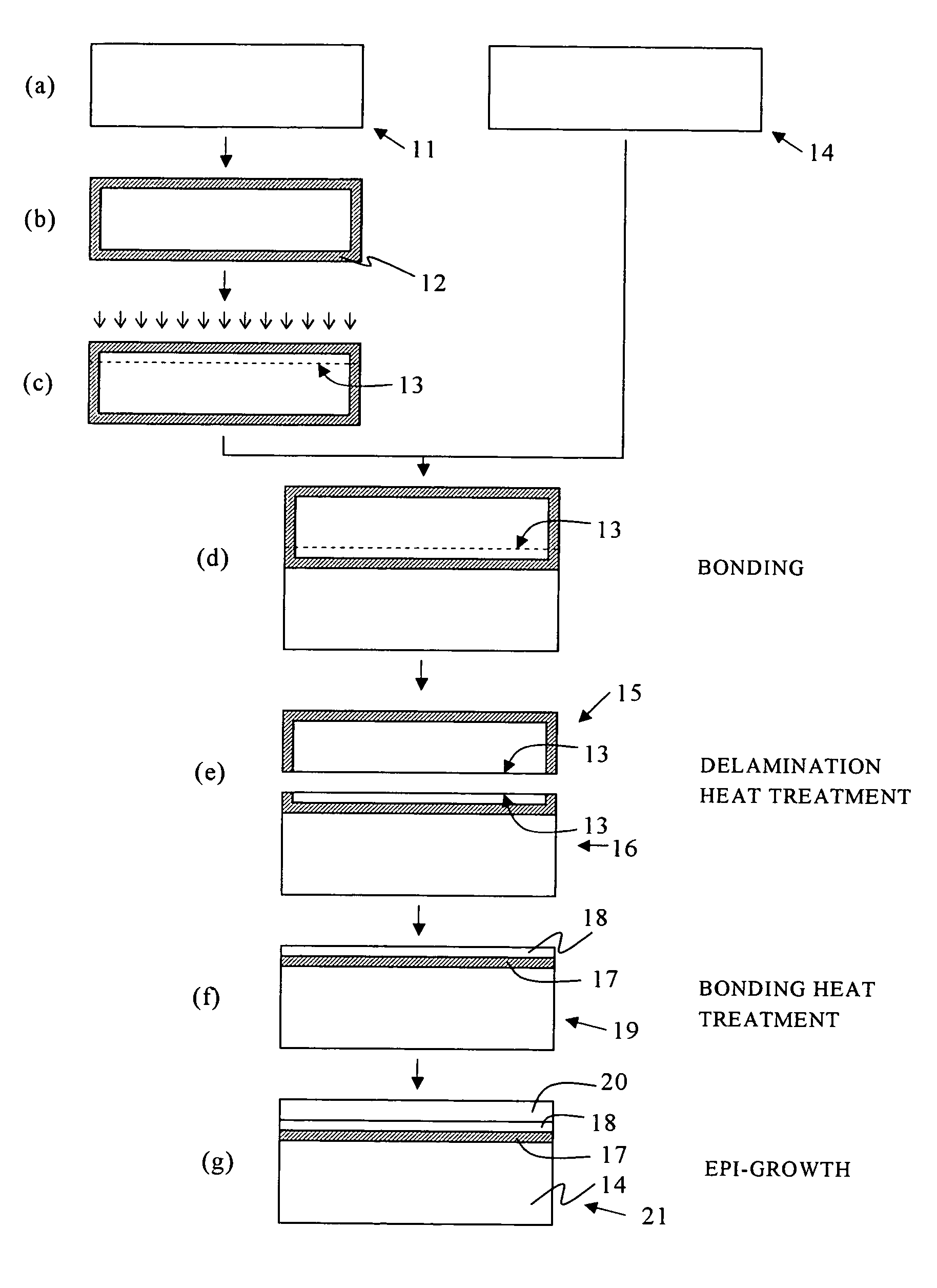
A method for fabricating an SOI wafer serving as a substrate based on the ion implantation delamination method will now be explained with reference to FIG. 1.

Four thin discoid wafers each formed of a CZ silicon single crystal substrate (a diameter: 200 mm (8 inches), a thickness: 625 μm) having an oxygen concentration of 20 ppma were prepared, and two wafers were determined as bond wafers whilst two wafers were determined as base wafers.

Then, the two bond wafers were subjected to a heat treatment in an oxidizing atmosphere to form an oxide film on an entire surface of each wafer. At this time, a time of the heat treatment was adjusted to set a thickness of the oxide film to 145 nm. A hydrogen ion was implanted into each of the two bond wafers under conditions where an implantation depth was set to 195 nm or 215 nm by d...


PUM


Abstract

The present invention provides a method for manufacturing an SOI wafer in which a thickness of an SOI layer is increased by growing an epitaxial layer on the SOI layer of the SOI wafer having an oxide film and the SOI layer formed on a base wafer, wherein the epitaxial growth is performed in such a manner that a reflectivity of a surface of the SOI wafer on which the epitaxial layer is grown in a wavelength region of a heating light at the start of the epitaxial growth falls within the range of 30% to 80%. As a result, in the method for manufacturing the SOI wafer in which a thickness of the SOI layer is increased by growing the epitaxial layer on the SOI layer of the SOI wafer having the oxide film and the SOI layer formed on the base wafer, a method for manufacturing a high-quality SOI wafer with less slip dislocation and others is provided.

Description

TECHNICAL FIELDThe present invention relates to a method for manufacturing an SOI wafer in which a thickness of an SOI layer is increased by subjecting a semiconductor single crystal film to the epitaxial growth on the SOI wafer serving as a substrate.BACKGROUND ARTAs a semiconductor substrate for a high-performance device, a bonded substrate obtained by bonding a bond wafer to a base wafer and then reducing a film thickness of the bond wafer is used. As one of such bonded substrates, an SOI substrate formed of silicon is known.As a method for manufacturing an SOI substrate, the following bonding method is known, for example. That is, two mirror-polished silicon wafers (a bond wafer and a base wafer) are prepared, and an oxide film is formed on at least one of the wafers. Further, these wafers are bonded to each other through the oxide film, and then a heat treatment is performed to increase bonding strength. Thereafter, a film thickness of the bond wafer is reduced to obtain an SOI...

Claims


Application Information

Patent Timeline
Patent Type & Authority Patents(United States)
IPC IPC(8): H01L21/30H01L21/46H01L21/76
CPCH01L21/76254H01L21/20
Inventor YAGI, SHINICHIRO
Owner SHIN-ETSU HANDOTAI CO LTD
Why Eureka
Try Eureka