Method and apparatus for detecting spatially varying and time-dependent magnetic fields

a spatially varying and time-dependent magnetic field technology, applied in the field of two-dimensional (2d) hall sensor array, can solve the problems of limited position resolution, slow and time-consuming process, and serious drawbacks of mos hall effect devices

Active Publication Date: 2011-03-08
MAGCAM
View PDF7 Cites 25 Cited by
  • Summary
  • Abstract
  • Description
  • Claims
  • Application Information

AI Technical Summary

Benefits of technology

[0012]The spatial resolution of a 2D Hall sensor array is related to both the size of the sensitive part of the Hall sensors, which is preferably between 100 nm and 1 mm, and the distance between two neighbouring Hall sensors

Problems solved by technology

Such scans are sequential by definition and therefore are slow and time-consuming processes.
Positioning of a magnetic object, for example, such as a permanent magnet, is currently being performed with a limited number (one or two) of individual Hall sensors, resulting in a limited position resolution.
However, MOS Hall effect devices have some serious drawbacks: the c

Method used


Image

  • Method and apparatus for detecting spatially varying and time-dependent magnetic fields
  • Method and apparatus for detecting spatially varying and time-dependent magnetic fields
  • Method and apparatus for detecting spatially varying and time-dependent magnetic fields

Examples


example 1

Working Principle

Semiconductor Material

[0101]The Hall sensors and switches are made from semiconductor material. This can be silicon, GaAs, InAs, InSb or an epitaxially grown III-V (or other) semiconductor heterostructure in which the heterojunction is made between a low band gap and a high band gap material such as GaAs / AlGaAs or GaN / AlGaN. In the case of semiconductor heterostructures, charge carriers (electrons) are provided to the semiconductor by a delta-doping layer (e.g. Si) in the case of GaAs / AlGaAs and by piezoelectric charges induced by the strained pseudomorphic epitaxy of AlGaN on GaN in the case of GaN / AlGaN. The electric fields inside the semiconductor induce a band bending which results in the formation of a quantum well at the heterojunction. The electrons are trapped in this quantum well and form a two-dimensional electron gas (2DEG) with high mobility at the position of the heterojunction. Mobilities in GaAs / AlGaAs range from more than 104 cm2 / Vs at room temperatu...

example 2

Processing

[0141]The processing of these two-dimensional Hall sensor array devices takes place in a cleanroom equipped with lithography facilities. The subsequent processing steps are best done by optical or electron beam lithography, but any other appropriate technique might as well be used.

[0142]The compatibility of semiconductor (preferably GaAs / AlGaAs or silicon) switches (preferably HMT or MOS transistors) with Hall sensors in the same material allows for a straightforward process flow.

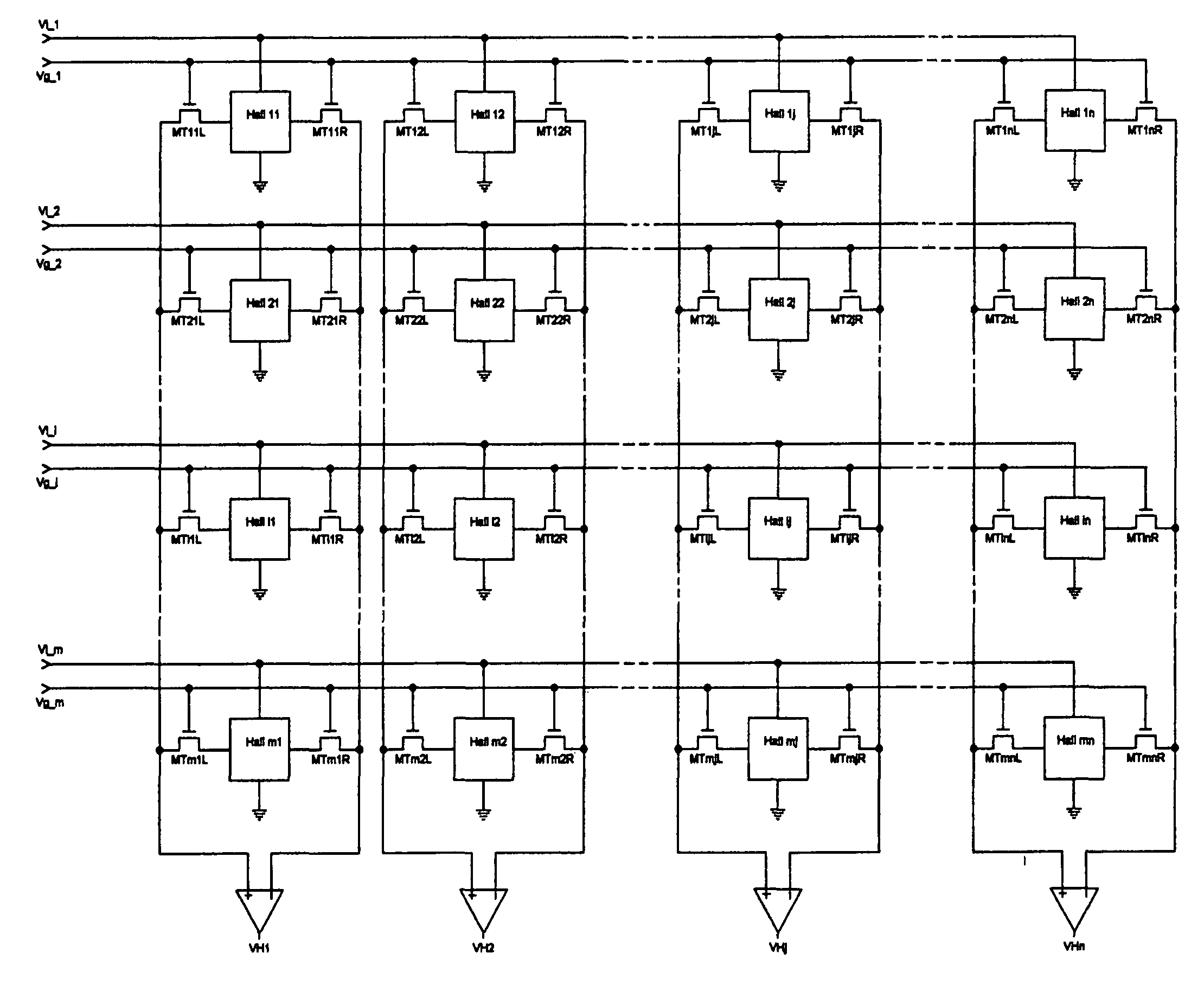
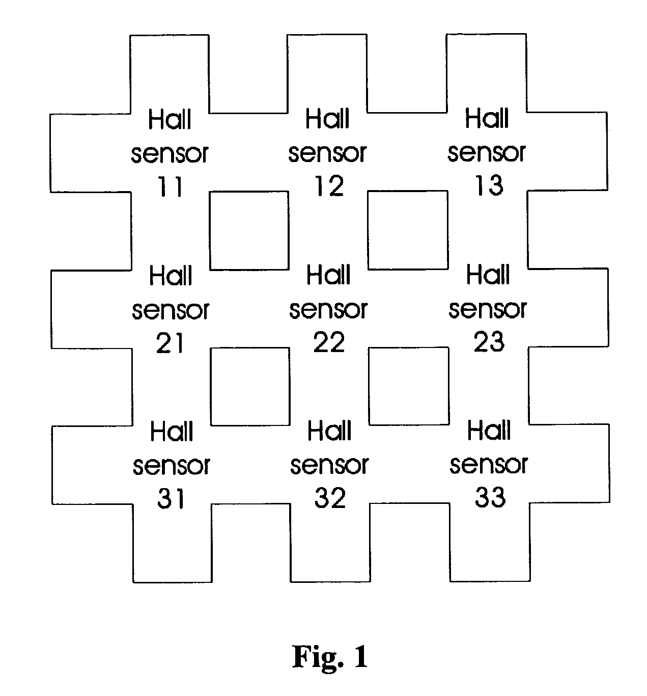
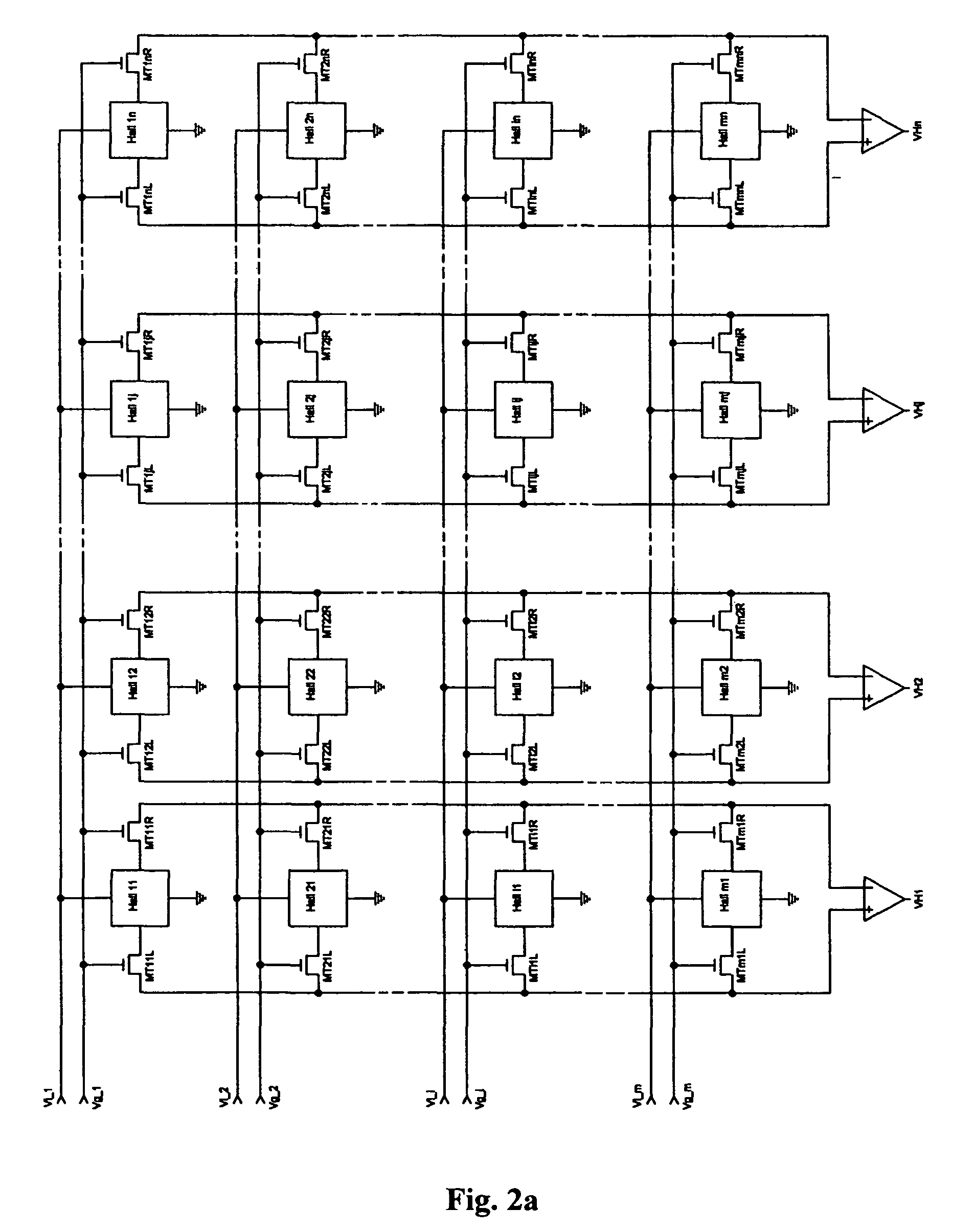
[0143]The Hall sensors are preferably cross-shaped. Geometrically, a cross is constructed by intersecting two orthogonal bars, as shown in FIG. 21. A cross has four arms, as indicated in FIG. 8. The terms ‘bar’ and ‘arm’ in the text are used according to these definitions. Making use of this cross-shape, we were able to develop a very compact design, using the left and right arm (corresponding to the Lij and Rij contacts respectively, see FIG. 8) of each Hall sensor (i,j) cross as MTijL and MTijR ...

example 3

Apparatus

[0160]A two-dimensional Hall sensor array chip (FIG. 9) has been developed and successfully tested. This prototype was processed from a delta doped GaAs / AlGaAs wafer. The chip contains several two-dimensional Hall sensor arrays of varying dimensions ranging from 1×1 (single Hall sensor) to 10×10, as well as single HEMT transistors.

[0161]The gate dielectric is a 10 nm thick Al2O3 oxide. The passivation layer is a 100 nm thick SiO2 layer.

[0162]Several tests have been done in order to characterize these devices. Their results demonstrate the successful operation of the two-dimensional Hall sensor array.

Transistor Characterization

[0163]Individual HEMT transistors have been tested and characterized. FIG. 10 shows the drain-source current and the gate leakage current as a function of the gate-source voltage with constant VDS between 0.5V and 2V. For VGS=0V, the transistor channel is conducting. For VGST, the drain-source current has dropped several orders of magnitude and the res...


PUM


Abstract

Certain inventive aspects provide local field imaging with high spatial, time and field resolution by using an array of Hall effect sensors that can be individually read out. The design combines semiconductor Hall sensors and switches that isolate the addressed Hall sensor from the rest of the array. The compact design allows for large and very dense Hall sensor arrays that can be read out in a straightforward way.

Description

BACKGROUND OF THE INVENTION[0001]1. Technical Field of the Invention[0002]The field relates generally to a two-dimensional (2D) Hall sensor array with high spatial, magnetic field and time resolution, for detecting spatially varying and time-dependent magnetic fields and, more particularly, to a system and method for individually addressing Hall sensors from a plurality of integrated Hall sensors and perceiving their individual response to a magnetic environment for magnetic field mapping, more particularly for high-precision positioning and magnetic field detection and imaging of magnetic field variations in time or in space.[0003]2. Description of the Related Technology[0004]Existing magnetic field detecting devices based on SQUID, GMR and Hall effect sensors are currently available only as individual sensors or one-dimensional arrays. This inevitably involves the need of either two-dimensional or one-dimensional scans if the spatial variation of the local magnetic field over a tw...

Claims


Application Information

Patent Timeline
IPC IPC(8): G01R33/07G01B7/14
CPCG01R33/0094G01R33/07G01R33/10
Inventor VERVAEKE, KOENBORGHS, GUSTAAFMOSHCHALKOV, VICTOR V.
Owner MAGCAM
Why Eureka
Try Eureka