Group III-nitride semiconductor crystal and manufacturing method thereof, and group III-nitride semiconductor device

a semiconductor crystal and manufacturing method technology, applied in the direction of crystal growth process, monocrystalline material growth, semiconductor lasers, etc., can solve the problems of insufficient light emission device drive voltage, inability to provide an electrode on the back surface, etc., to achieve efficient manufacturing method, small absorption coefficient, and high light emission intensity

Active Publication Date: 2011-03-15
SUMITOMO ELECTRIC IND LTD +1
View PDF16 Cites 8 Cited by
  • Summary
  • Abstract
  • Description
  • Claims
  • Application Information

AI Technical Summary

Benefits of technology

[0019]As described above, according to the present invention, group III-nitride semiconductor crystal attaining a small absorption coefficient and an efficient method of manufacturing the same, as well as a group III-nitride semiconductor device attaining high light emission intensity can be provided.

Problems solved by technology

As the sapphire substrate attains high insulation, it is not possible to provide an electrode on a back surface of the sapphire substrate (referring to a surface of the substrate where a semiconductor layer having a light emission layer is not formed, hereinafter the same as above).
In such a case, as a result of a current passing through the semiconductor layer having a small thickness, a drive voltage of a light emission device has undesirably been high.
The absorption coefficient of that GaN crystal substrate, however, is not sufficiently small (see, for example, Japanese Patent Laying-Open No. 2000-12900 (Patent Document 1)).
The GaN crystal substrate obtained through the flux method, however, is also colored orange or brown, and the absorption coefficient of that GaN crystal substrate is not sufficiently small (see, for example, Hisanori Yamane, et al., “GaN Single Crystal Growth by the Flux Method,” Oyo Buturi, The Japan Society of Applied Physics, May, 2002, Vol. 71, No. 5, pp.
This may be because metal Na representing an alkali-metal-element-containing substance is highly susceptible to oxidation, i.e., an oxygen atom or the like is introduced as an impurity atom, and therefore it is difficult to obtain high-purity group III-nitride semiconductor crystal.

Method used


Image

  • Group III-nitride semiconductor crystal and manufacturing method thereof, and group III-nitride semiconductor device
  • Group III-nitride semiconductor crystal and manufacturing method thereof, and group III-nitride semiconductor device
  • Group III-nitride semiconductor crystal and manufacturing method thereof, and group III-nitride semiconductor device

Examples


embodiment 1

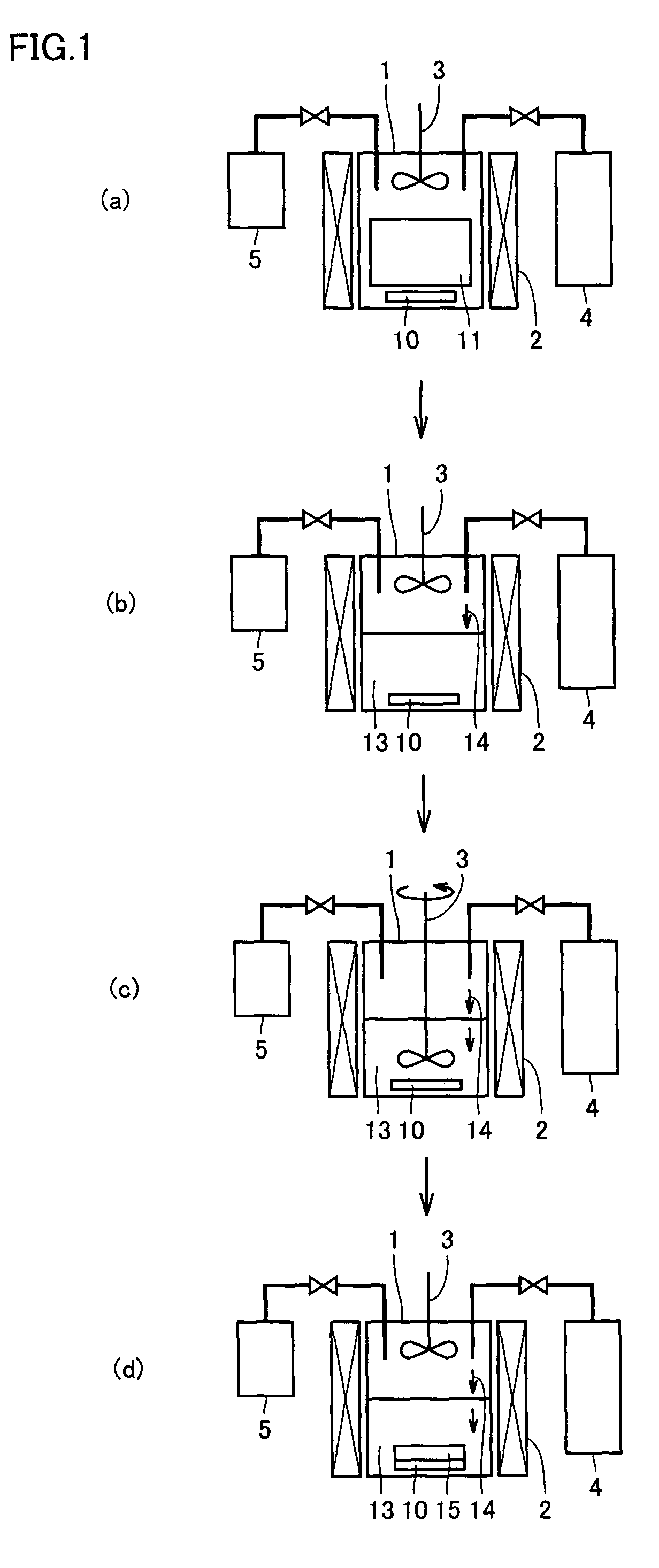
[0031]Referring to FIG. 1, a method of manufacturing group III-nitride semiconductor crystal according to the present invention includes the steps of: accommodating an alloy 11 containing at least a group III-metal element and an alkali metal element in a reactor 1; introducing a nitrogen-containing substance 14 in reactor 1; dissolving nitrogen-containing substance 14 in an alloy melt 13 in which alloy 11 has been melted; and growing group III-nitride semiconductor crystal 15.

[0032]By accommodating alloy 11 containing at least the group III-metal element and the alkali metal element in the reactor, introduction of an oxygen atom (hereinafter referred to as O atom) into the group III-nitride semiconductor crystal is suppressed, as compared with a case in which an alkali-metal-element-containing substance susceptible to oxidation is directly accommodated in the reactor. Therefore, the group III-nitride semiconductor crystal attaining a small absorption coefficient is obtained.

[0033]I...

embodiment 2

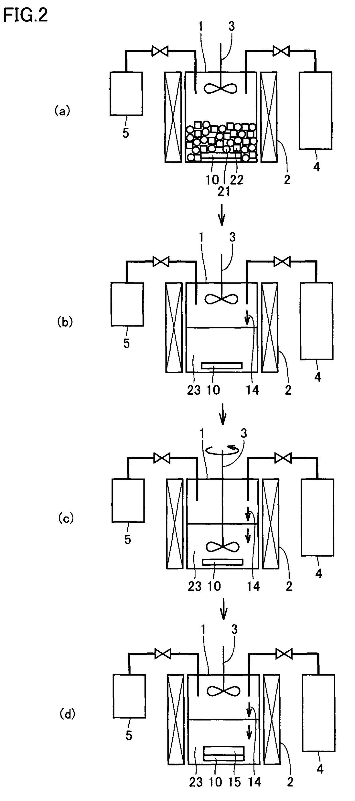
[0043]Referring to FIG. 2, another method of manufacturing group III-nitride semiconductor crystal according to the present invention includes the steps of: accommodating at least a group III-metal-element-containing substance 21 and an alkali-metal-element-containing substance 22 in reactor 1; introducing nitrogen-containing substance 14 in reactor 1; stirring a melt 23 in which group III-metal-element-containing substance 21 and alkali-metal-element-containing substance 22 have been melted; dissolving nitrogen-containing substance 14 in melt 23; and growing group III-nitride semiconductor crystal 15. Melt 23 is forcibly stirred, so that the group III-metal element atoms and the alkali metal element atoms in melt 23 can be mixed well and dissolution of nitrogen-containing substance 14 into melt 23 is promoted. Therefore, a time until the group III-nitride semiconductor crystal starts to grow and a time for growth can be shortened. In addition, as a result of a shorter time until th...

embodiment 3

[0048]Referring to FIG. 4, the group III-nitride semiconductor device according to the present invention implements an LED, in which an n-type GaN layer 41, an In0.2Ga0.8N layer 42, an Al0.2Ga0.8N layer 43, and a p-type GaN layer 44 are successively formed as the group III-nitride crystal semiconductor layer on a group III-nitride semiconductor crystal substrate 40 implemented by the group III nitride semiconductor crystal, a p-side electrode 45 is formed on an upper surface of p-type GaN layer 44, and an n-side electrode 66 is formed in the center of a lower surface of group III-nitride semiconductor crystal substrate 40. The group III-nitride semiconductor device gives off light emission 50. The group III-nitride semiconductor device employing the group III-nitride semiconductor crystal substrate that attains an absorption coefficient, in a wavelength range from 375 nm to 500 nm, of at most 50 cm−1 attains improved light emission intensity.


PUM

PropertyMeasurementUnit
temperatureaaaaaaaaaa
absorption coefficientaaaaaaaaaa
temperatureaaaaaaaaaa

Abstract

A method of manufacturing group III-nitride semiconductor crystal includes the steps of accommodating an alloy containing at least a group III-metal element and an alkali metal element in a reactor, introducing a nitrogen-containing substance in the reactor, dissolving the nitrogen-containing substance in an alloy melt in which the alloy has been melted, and growing group III-nitride semiconductor crystal is provided. The group III-nitride semiconductor crystal attaining a small absorption coefficient and an efficient method of manufacturing the same, as well as a group III-nitride semiconductor device attaining high light emission intensity can thus be provided.

Description

RELATED APPLICATIONS[0001]This application is the U.S. National Phase under 35 U.S.C. §371 of International Application No. PCT / JP2005 / 006076, filed on Mar. 30, 2005, which in turn claims the benefit of JP 2004-148923, filed on May 19, 2004, the disclosures of which Applications are incorporated by reference herein.TECHNICAL FIELD[0002]The present invention relates to group III-nitride semiconductor crystal attaining a small absorption coefficient and an efficient method of manufacturing the same, as well as to a group III-nitride semiconductor device attaining high light emission intensity.BACKGROUND ART[0003]A sapphire substrate, a GaN substrate or the like is used as a substrate for a semiconductor device such as a light emitting diode (hereinafter referred to as LED) or a laser diode (hereinafter referred to as LD).[0004]As the sapphire substrate attains high insulation, it is not possible to provide an electrode on a back surface of the sapphire substrate (referring to a surfac...

Claims


Application Information

Patent Timeline
Patent Type & Authority Patents(United States)
IPC IPC(8): C30B21/02C30B9/12C30B11/00C30B11/06C30B29/38C30B29/40H01L21/208H01L33/00H01S5/323
CPCC30B9/12C30B11/00C30B29/403H01L33/0075H01L21/02625H01L21/02392H01L21/0242H01L21/02458H01L21/0254H01L21/02389H01S5/32341
Inventor SASAKI, TAKATOMOMORI, YUSUKEYOSHIMURA, MASASHIKAWAMURA, FUMIONAKAHATA, SEIJIHIROTA, RYU
Owner SUMITOMO ELECTRIC IND LTD
Why Eureka
Try Eureka