Dry etching method, fine structure formation method, mold and mold fabrication method
a technology of fine structure and etching method, which is applied in the direction of optical waveguide light guide, optical element, transportation and packaging, etc., can solve the problems of rigidity and durability, inability to reduce the cost of optical waveguide, and inability to meet the requirements of machining method, etc., to achieve the effect of improving the etching efficiency of tungsten by halogen, low volatility and high volatility
- Summary
- Abstract
- Description
- Claims
- Application Information
AI Technical Summary
Benefits of technology
Problems solved by technology
Method used
Image
Examples
embodiment 1
[0131]A dry etching method according to Embodiment 1 of the invention will now be described with reference to the accompanying drawings.
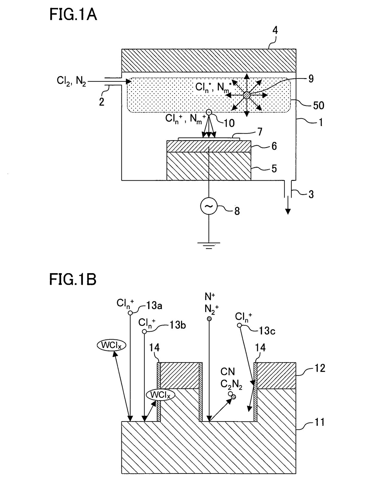
[0132]FIGS. 1(a) and 1(b) are explanatory diagrams of the dry etching method of Embodiment 1 of the invention. As shown in FIG. 1(a), a reaction chamber 1 in which a reduced pressure can be kept is provided with a gas inlet 2 and a gas outlet 3. Also, a plasma generator 4 for changing a gas supplied through the gas inlet 2 into plasma is provided in an upper portion of the reaction chamber 1. Furthermore, an electrode 6 on which a target substance including tungsten and carbon, specifically, a WC alloy substrate or a substrate having a WC alloy in its surface portion (hereinafter both referred to as a WC substrate 7), is placed is provided on an insulator 5 in a lower portion of the reaction chamber 1. An RF (radio frequency) power source 8 for applying a bias voltage to the electrode 6 is provided outside the reaction chamber 1.
[0133]Next, the oper...
embodiment 2
[0145]Now, a dry etching method according to Embodiment 2 of the invention will be described with reference to the accompanying drawings. A difference of the dry etching method of this embodiment from that of Embodiment 1 is that a substance including tungsten and carbon as principal compositions is dry etched by using plasma generated from a gas made by additionally adding a gas including a hydrogen atom to a mixed gas of a gas including a chlorine atom and a gas including a nitrogen atom.
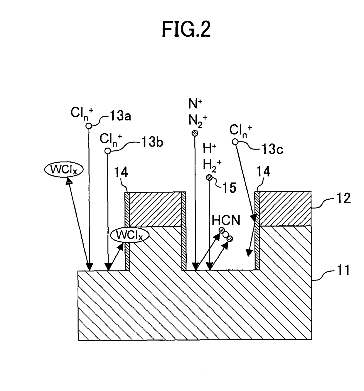
[0146]FIG. 2 is an explanatory diagram of the dry etching method according to Embodiment 2 of the invention. Hereinafter, the dry etching method of this embodiment will be described by exemplifying the case where a chlorine molecule, a nitrogen molecule, and a hydrogen molecule are used as the gas including a chlorine atom, the gas including a nitrogen atom, and the gas including a hydrogen atom, respectively.
[0147]Referring to FIG. 2, in this embodiment, a resist pattern 12 is formed on a WC subs...
embodiment 3
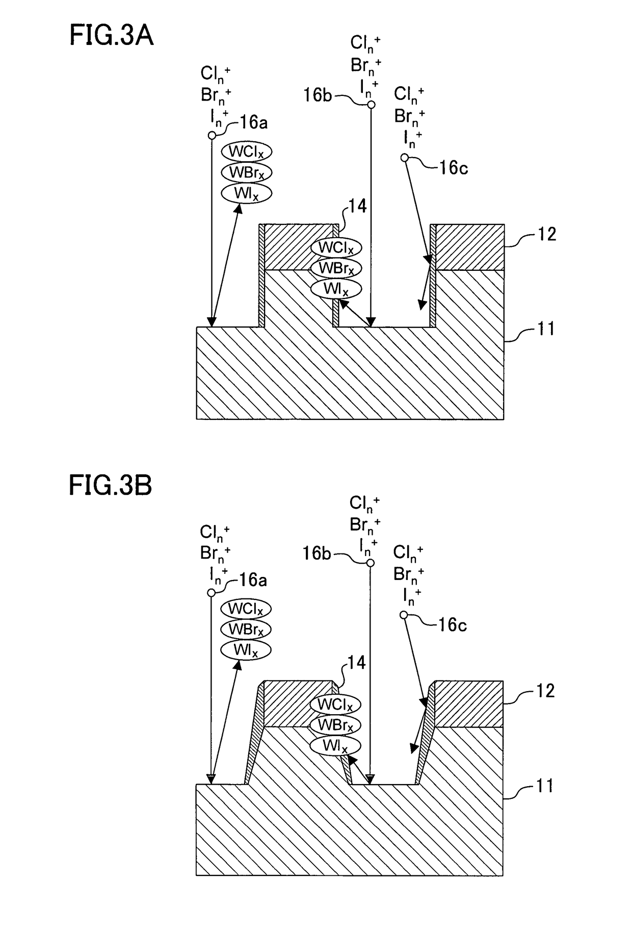
[0157]Now, a dry etching method according to Embodiment 3 of the invention will be described with reference to the accompanying drawings. A difference of the dry etching method of this embodiment from that of Embodiment 1 is that a substance including tungsten and carbon as principal components is dry etched by using plasma generated from a gas which is made by additionally mixing at least one of a gas including a bromine atom and a gas including an iodine atom into a mixed gas of a gas including a chlorine atom and a gas including a nitrogen atom.
[0158]FIGS. 3(a) and 3(b) are explanatory diagrams of the dry etching method of Embodiment 3 of the invention, in each of which a state of a WC substrate being etched by the dry etching method is shown. It is noted that FIG. 3(a) shows a case where a sidewall protecting film is formed in a small thickness and FIG. 3(b) shows a case where a sidewall protecting film is formed in a large thickness. Now, the dry etching method of this embodime...
PUM
| Property | Measurement | Unit |
|---|---|---|
| boiling point | aaaaa | aaaaa |
| boiling points | aaaaa | aaaaa |
| boiling points | aaaaa | aaaaa |
Abstract
Description
Claims
Application Information


