GaN crystal substrate, fabricating method of GaN crystal substrate, and light-emitting device

a technology of gan crystal substrate and gan crystal substrate, which is applied in the direction of crystal growth process, polycrystalline material growth, chemically reactive gas growth, etc., can solve the problems of degrading optical output and inability to form an electrode on the back surface, and achieves small light absorption coefficient and increased optical output

Active Publication Date: 2011-04-19
SUMITOMO ELECTRIC IND LTD
View PDF7 Cites 6 Cited by
  • Summary
  • Abstract
  • Description
  • Claims
  • Application Information

AI Technical Summary

Benefits of technology

[0007]Meanwhile, in the case where a conductive GaN crystal substrate, such as an n-type GaN crystal substrate, is used as the substrate for a light-emitting device, it is possible to form the electrode on the back surface of the GaN crystal substrate having a large cross section, and thus, the driving voltage of the light-emitting device can be reduced compared to the case of using the sapphire substrate.
[0011]In view of the foregoing, an object of the present invention is to provide a GaN crystal substrate having a small absorption coefficient of light, a fabricating method of the GaN crystal substrate, and a light-emitting device increased in optical output that is fabricated using the GaN crystal substrate.
[0018]According to the present invention, it is possible to provide a GaN crystal substrate having a small absorption coefficient of light, a fabricating method of the GaN crystal substrate, and a light-emitting device increased in optical output that is fabricated using the GaN crystal substrate.

Problems solved by technology

In the case where a sapphire substrate is used as the substrate for a light-emitting device, it is not possible to form an electrode on a back surface of the sapphire substrate (opposite to the surface (growth surface) on which semiconductor layers including a light-emitting layer are grown), due to high insulating property of the sapphire substrate.
This would degrade the optical output.

Method used


Image

  • GaN crystal substrate, fabricating method of GaN crystal substrate, and light-emitting device
  • GaN crystal substrate, fabricating method of GaN crystal substrate, and light-emitting device
  • GaN crystal substrate, fabricating method of GaN crystal substrate, and light-emitting device

Examples


example 1

[0051]1. Fabrication of GaN Crystal Substrate

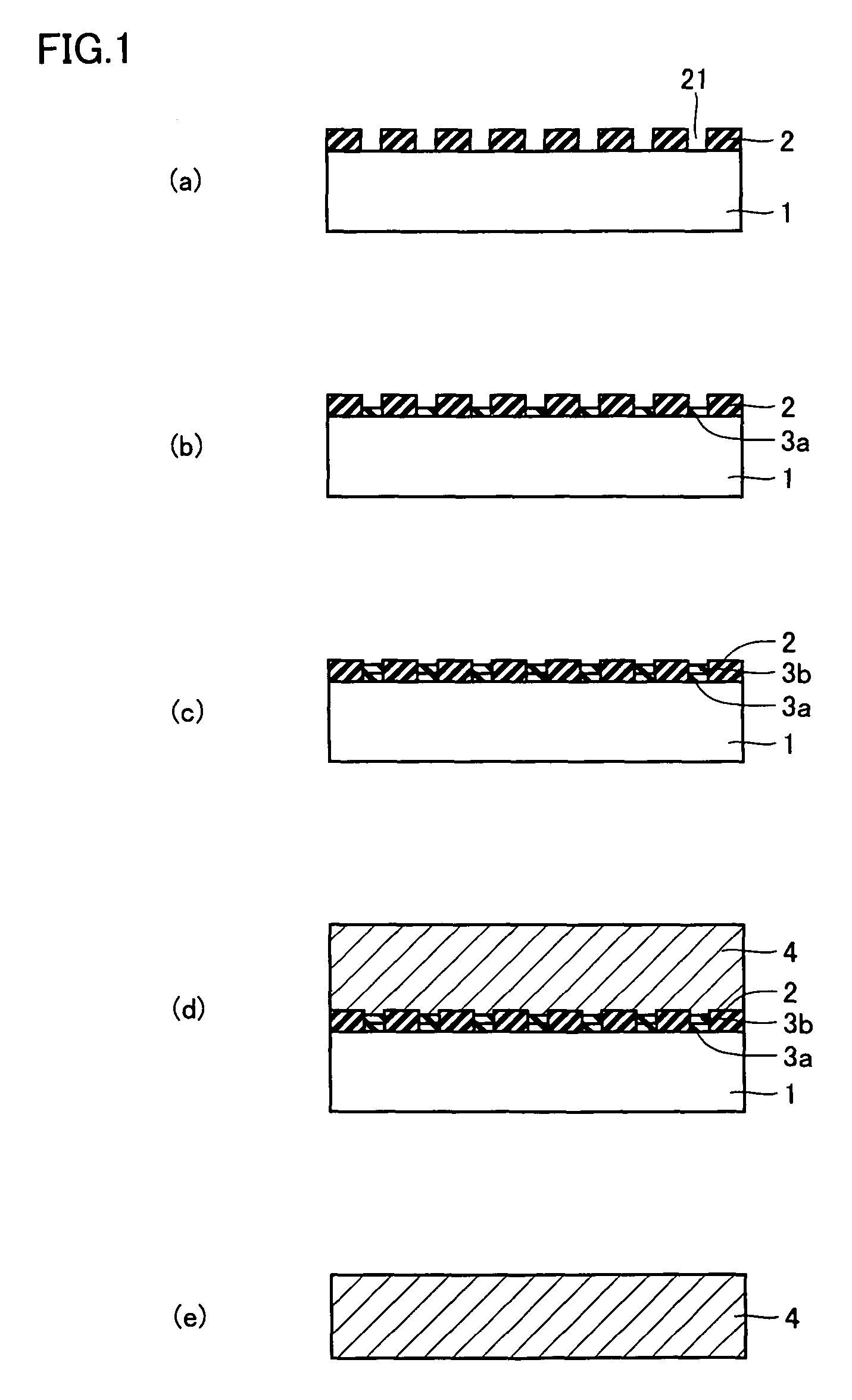
[0052]Firstly, on a GaAs substrate 1 having a diameter of 50 mm, a Si3N4 layer having a thickness of 100 nm was formed as a mask layer 2 by CVD under the atmospheric pressure, as shown in FIG. 1(a).

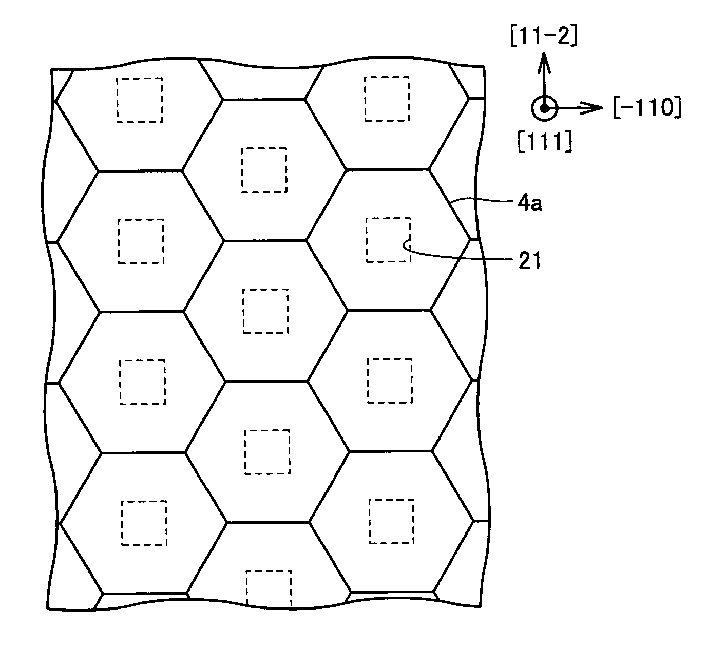
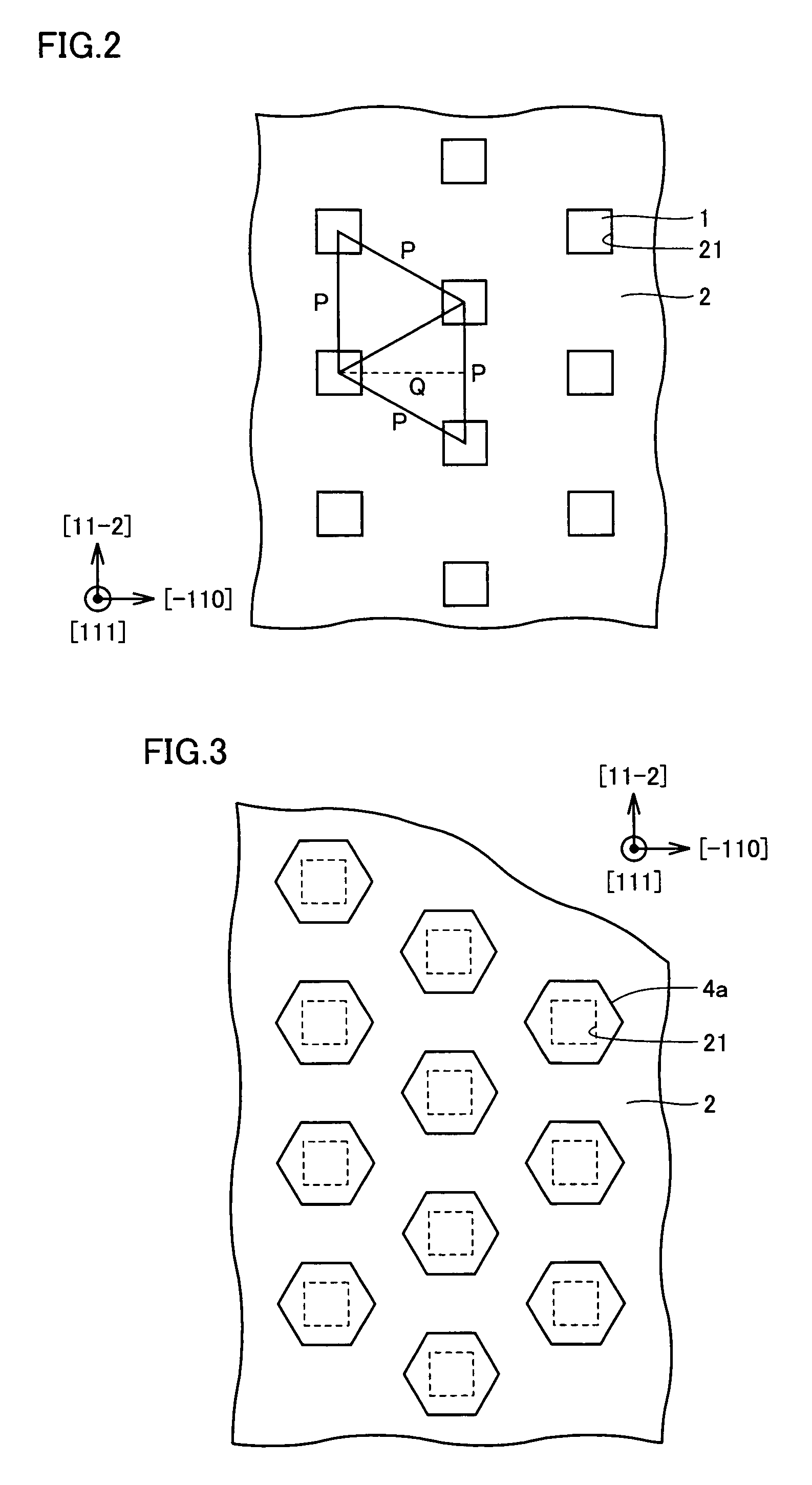
[0053]Thereafter, openings 21 were formed at mask layer 2 by photo etching to have centers corresponding to apexes of triangles with P of 4 μm and Q of 3.5 μm shown in FIG. 2. Here, opening 21 was shaped into a quadrate with a side of 1 μm.

[0054]Next, as shown in FIG. 1(b), a first GaN buffer layer 3a was grown to a thickness of 40 nm on the surface of GaAs substrate 1 exposed from openings 21 by HVPE, using HCl gas (partial pressure: 60.8 Pa) and NH3 gas (partial pressure: 1.31×10⁴ Pa) as the source gases, at the ambient temperature of 475° C.

[0055]Subsequently, as shown in FIG. 1(c), a second GaN buffer layer 3b was grown to a thickness of 40 nm on first GaN buffer layer 3a by HVPE, using HCl gas (partial pressure: 60.8 Pa) and NH3 gas (parti...

example 2

[0070]A GaN crystal substrate of Example 2 was fabricated in a similar manner and under similar conditions as in Example 1, except that mixed gas of O2 and N2 (partial pressure: 6.55×10² Pa) containing 0.1 mass % of O2 as well as HCl gas (partial pressure: 1.25×10³ Pa) and NH3 gas (partial pressure: 1.31×10⁴ Pa) were used as the source gases. The surface of the GaN crystal substrate of Example 2 had surface roughness Ra of 3 nm.

[0071]For the GaN crystal substrate of Example 2 thus obtained, the carrier concentration and the light absorption coefficient were evaluated in a similar manner and under similar conditions as in Example 1. The results are shown in Table 1.

[0072]As shown in Table 1, the GaN crystal substrate of Example 2 had the carrier concentration of 2×1019 cm−3, and the absorption coefficient of light of 375 nm wavelength was 68 cm−1, and the absorption coefficient of light of 500 nm wavelength was 10 cm−1. Since the light absorption coefficient becomes greater as the wa...

example 3

[0075]A GaN crystal substrate of Example 3 was fabricated in a similar manner and under similar conditions as in Example 1, except that mixed gas of SiH4 and N2 (partial pressure: 93.5 Pa) containing 0.1 mass % of SiH4 as well as HCl gas (partial pressure: 1.25×10³ Pa) and NH3 gas (partial pressure: 1.31×10⁴ Pa) were used as the source gases. The surface of the GaN crystal substrate of Example 3 had surface roughness Ra of 3 nm.

[0076]For the GaN crystal substrate of Example 3 thus obtained, the carrier concentration and the light absorption coefficient were evaluated in a similar manner and under similar conditions as in Example 1. The results are shown in Table 1.

[0077]As shown in Table 1, the GaN crystal substrate of Example 3 had the carrier concentration of 5×1017 cm−3, and the absorption coefficient of light of 375 nm wavelength was 35 cm−1, and the absorption coefficient of light of 500 nm wavelength was 8 cm−1. Since the light absorption coefficient becomes greater as the wav...


PUM

PropertyMeasurementUnit
light absorption coefficientaaaaaaaaaa

Abstract

A GaN crystal substrate is provided, which has a diameter of not less than 20 mm and a thickness of not less than 70 μm and not more than 450 μm, and has a light absorption coefficient of not less than 7 cm−1 and not more than 68 cm−1 for light in the wavelength range of not less than 375 nm and not more than 500 nm. A fabricating method of the GaN crystal substrate, and a light-emitting device fabricated using the GaN crystal substrate are also provided.

Description

BACKGROUND OF THE INVENTION[0001]1. Field of the Invention[0002]The present invention relates to a GaN (gallium nitride) crystal substrate, a fabricating method of the GaN crystal substrate, and a light-emitting device. More particularly, the present invention relates to a GaN crystal substrate having a small absorption coefficient of light, a fabricating method of the GaN crystal substrate, and a light-emitting device increased in optical output that is fabricated using the GaN crystal substrate.[0003]2. Description of the Background Art[0004]Currently, a sapphire substrate or a GaN crystal substrate is primarily used as a substrate for a light-emitting device such as a light-emitting diode (hereinafter, “LED”), a laser diode (hereinafter, “LD”) and the like.SUMMARY OF THE INVENTION[0005]In the case where a sapphire substrate is used as the substrate for a light-emitting device, it is not possible to form an electrode on a back surface of the sapphire substrate (opposite to the sur...

Claims


Application Information

Patent Timeline
Patent Type & Authority Patents(United States)
IPC IPC(8): H01L27/15
CPCC30B25/02C30B29/406C30B25/04H01L33/0075
Inventor MATSUOKA, TORUMOTOKI, KENSAKU
Owner SUMITOMO ELECTRIC IND LTD
Why Eureka
Try Eureka