

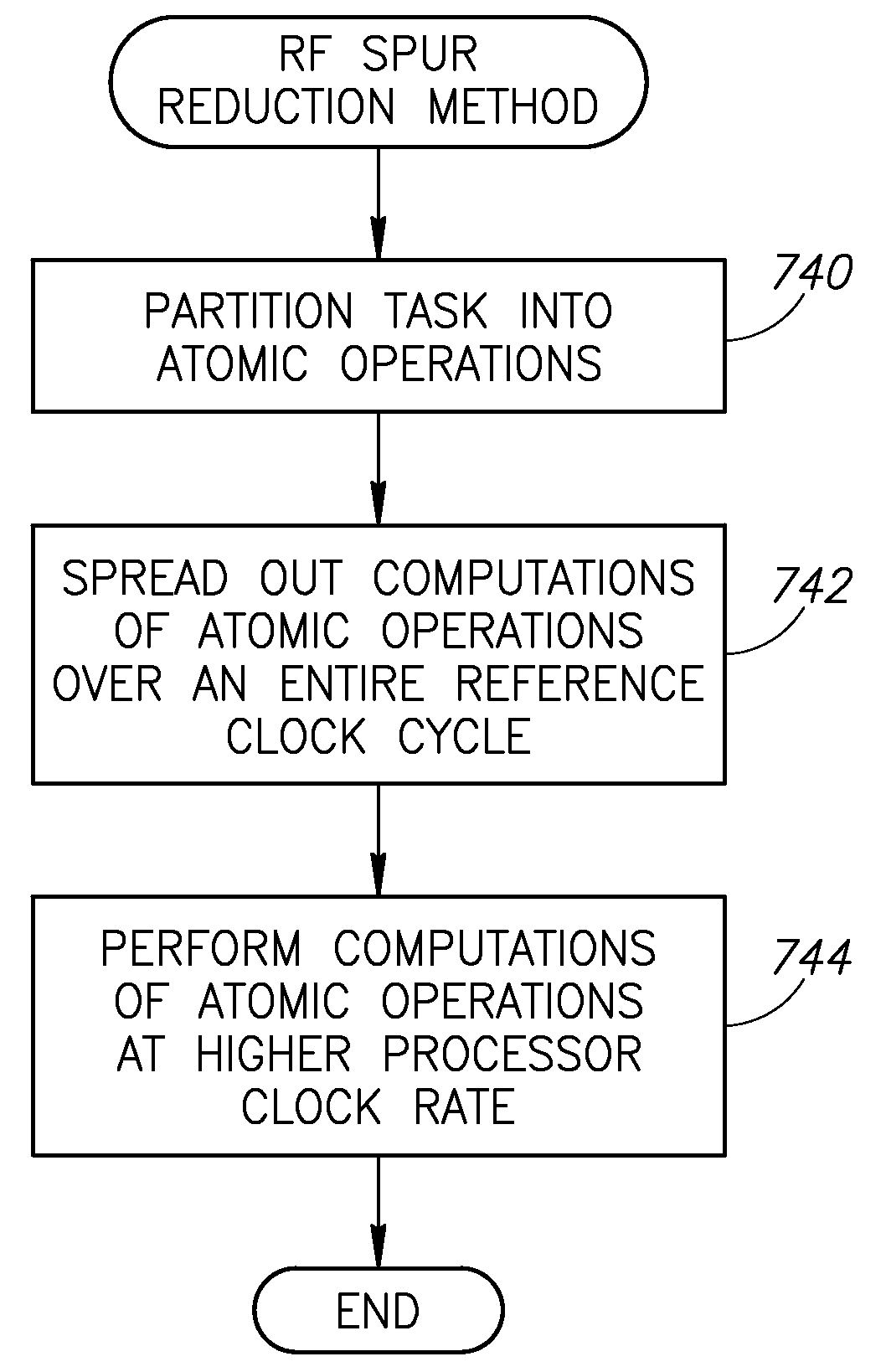
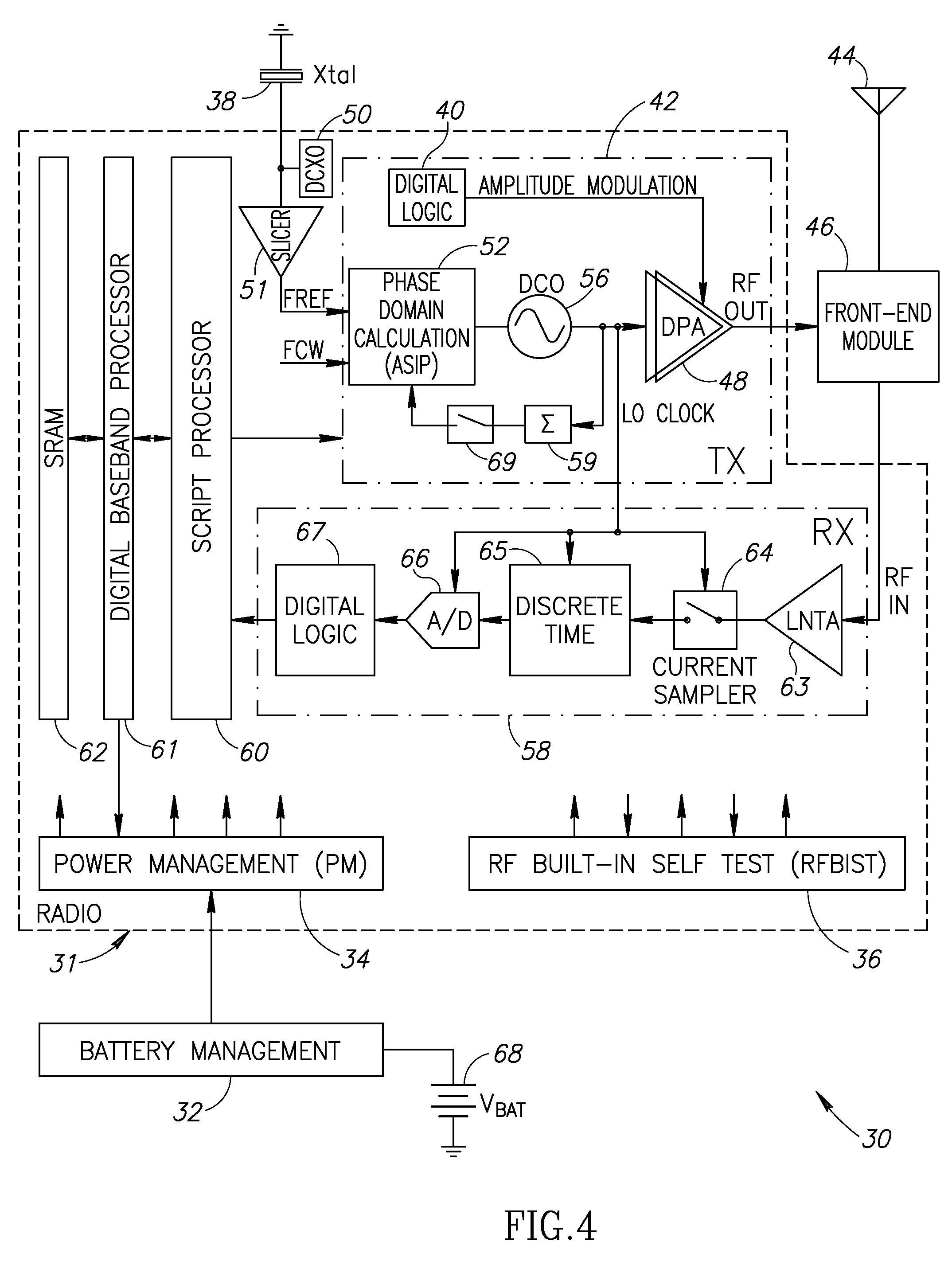
Computation spreading for spur reduction in a digital phase lock loop
a phase lock loop and computation spreading technology, applied in computation using denominational number representation, generating/distributing signals, instruments, etc., can solve the problems of difficult one design to support multi-standard wireless applications, many time-consuming steps, and limited reconfigurability of conventional adpll circuits, so as to reduce and reducing the effect of frequency spur generation
- Summary
- Abstract
- Description
- Claims
- Application Information
AI Technical Summary
Benefits of technology
Problems solved by technology
Method used
Image

Examples
Embodiment Construction
Notation Used Throughout
[0061]The following notation is used throughout this document.
[0062]
TermDefinitionACAlternating CurrentACLAsynchronous Connectionless LinkACWAmplitude Control WordADCAnalog to Digital ConverterADPLLAll Digital Phase Locked LoopALUArithmetic Logic UnitAMAmplitude ModulationASICApplication Specific Integrated CircuitASIPApplication Specific Instruction-set ProcessorAVIAudio Video InterfaceAWSAdvanced Wireless ServicesBISTBuilt-In Self TestBMPWindows BitmapBPFBand Pass FilterCMOSComplementary Metal Oxide SemiconductorCPUCentral Processing UnitCUControl UnitCWContinuous WaveDACDigital to Analog ConverterdBDecibelDBBDigital BasebandDCDirect CurrentDCODigitally Controlled OscillatorDCXODigitally Controlled Crystal OscillatorDPADigitally Controlled Power AmplifierDPLLDigital Phase Locked LoopDRACDigital to RF Amplitude ConversionDRPDigital RF Processor or Digital Radio ProcessorDSLDigital Subscriber LineDSPDigital Signal ProcessorEDGEEnhanced Data Rates for GSM Evol...
PUM
 Abstract
Description
Claims
Application Information