

Light emitting element and light emitting device
- Summary
- Abstract
- Description
- Claims
- Application Information
AI Technical Summary
Benefits of technology
Problems solved by technology
Method used
Image

Examples
example 1
[0086]In this example, a device configuration of a light emitting element and a method for manufacturing thereof according to the present invention will be explained with reference to FIG. 5.
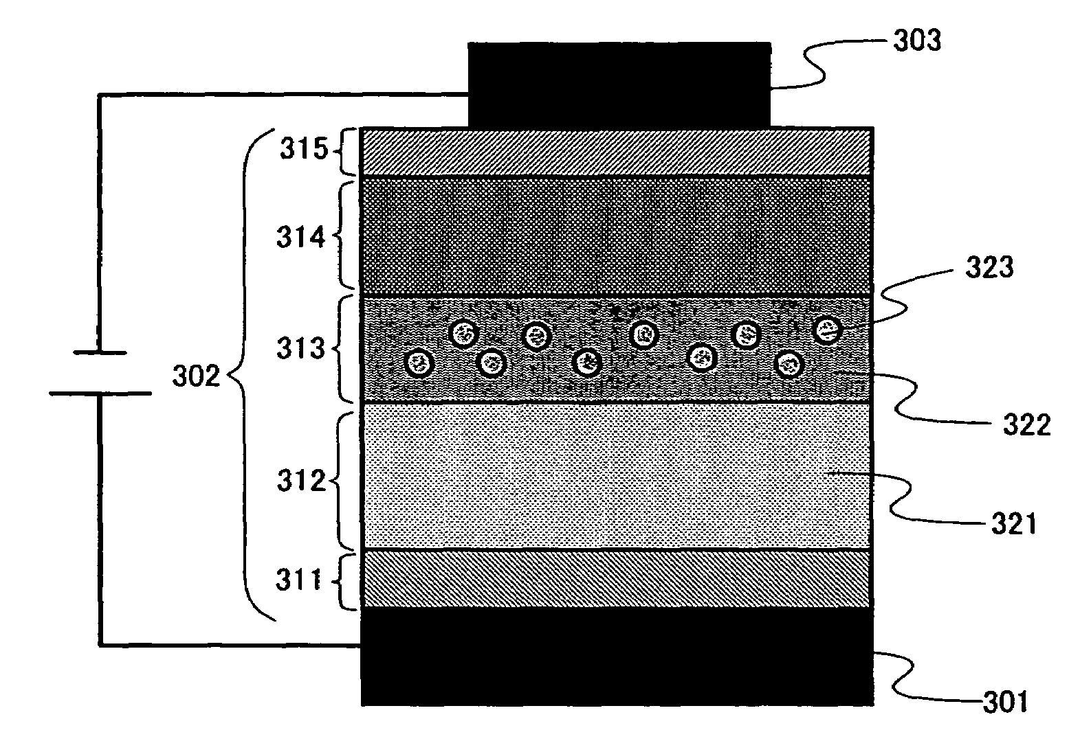
[0087]An anode 501 of the light emitting element is formed over a glass substrate 500 having an insulating surface. As a material for the anode 501, ITO, a transparent conductive film, is used. The anode 501 is formed by sputtering to have a thickness of 110 nm. The anode 501 is square in shape and 2 mm in height and width.
[0088]Then, an electroluminescent layer 502 is formed over the anode 501. In this example, the electroluminescent layer 502 has a lamination structure comprising a hole injecting layer 511; a first light emitting layer 512, which has hole injection properties; a second light emitting layer 513; an electron transporting layer 514; and an electron injecting layer 515. The first light emitting layer 512 is formed by a material, which can achieve blue emission, specifically, a mat...
example 2
[0097]In this example, device characteristics of the light emitting element described in Example 1 having the configuration: ITO / Cu-Pc (20 nm) / α-NPD (30 nm) / CBP+Pt(ppy)acac: 15 wt % (20 nm) / BCP (30 nm) / CaF (2 nm) / Al (100 nm) will be explained. Emission spectrum of the light emitting element having the above described configuration is shown by each spectrum 1 in FIG. 8 and FIG. 9. Each plot 1 in FIGS. 10 to 13 shows for electric characteristics.
[0098]Spectrum 1 in FIG. 8 shows the emission spectrum of the light emitting element having the above described configuration at an applied current of 1 mA (approximately 960 cd / m2). From the result shown by spectrum 1, white emission can be obtained having three components: blue emission from α-NPD composing the first light emitting layer (˜450 nm); green emission of phosphorescent light emission from Pt(ppy)acac contained in a second light emitting layer (˜490 nm, ˜530 nm); and orange emission from excimer light emission of Pt(ppy)acac conta...
example 3
[0113]In this example, a method for manufacturing a light emitting device (top emission structure) having a light emitting element according to the present invention, which exhibits white emission, over a substrate having an insulating surface will be explained with reference to FIG. 6. As used herein, the term “top emission structure” refers to a structure in which light is extracted from the opposite side of the substrate having an insulating surface.
[0114]FIG. 6A is a top view of a light emitting device. FIG. 6B is a cross-sectional view of FIG. 6A taken along the line A-A′. Reference numeral 601 indicated by a dotted line denotes a source signal line driver circuit; 602, a pixel portion; 603, a gate signal line driver circuit; 604, a transparent sealing substrate; 605, a first sealing agent; and 607, a second sealing agent. The inside surrounded by the first sealing agent 605 is filled with the transparent second sealing agent 607. In addition, the first sealing agent 605 contai...
PUM
| Property | Measurement | Unit |
|---|---|---|
| Percent by mass | aaaaa | aaaaa |
| Nanoscale particle size | aaaaa | aaaaa |
| Nanoscale particle size | aaaaa | aaaaa |
Abstract
Description
Claims
Application Information