
PVD-based metallization methods for fabrication of interconnections in semiconductor devices

Active Publication Date: 2011-06-21
NOVELLUS SYSTEMS
View PDF18 Cites 33 Cited by
  • Summary
  • Abstract
  • Description
  • Claims
  • Application Information

AI Technical Summary

Benefits of technology

[0013]The ability of depositing the metal within the recessed feature while simultaneously etching material from the field region or while depositing metal in the field region at a lower rate, is highly unusual for an iPVD method, which is conventionally characterized by an opposite deposition selectivity, that is, by higher deposition rates in the field compared to the recess bottom. Unexpectedly, the use of high density plasma characterized by high fractional ionization of metal, resulted in reversal of the selectivity and enabled bottom-up recess fill without formation of substantial overhangs at the recess opening.

Problems solved by technology

Filling of these recessed features with metals presents many challenges.
In particular, the difficulty of depositing metals into narrow recesses without forming microvoids or defects, has prevented the use of PVD methods for metal gap fill at a current level of miniaturization.
However, the goal of PVD-only metal fill has been difficult to attain.
With the use of conventional PVD in narrow and high aspect ratio features, the metal sputtered from the metal target tends to accumulate at the opening of the recessed feature, causing formation of overhangs, and, ultimately, leading to formation of voids within the filled feature.

Method used


Image

  • PVD-based metallization methods for fabrication of interconnections in semiconductor devices
  • PVD-based metallization methods for fabrication of interconnections in semiconductor devices
  • PVD-based metallization methods for fabrication of interconnections in semiconductor devices

Examples


first embodiment

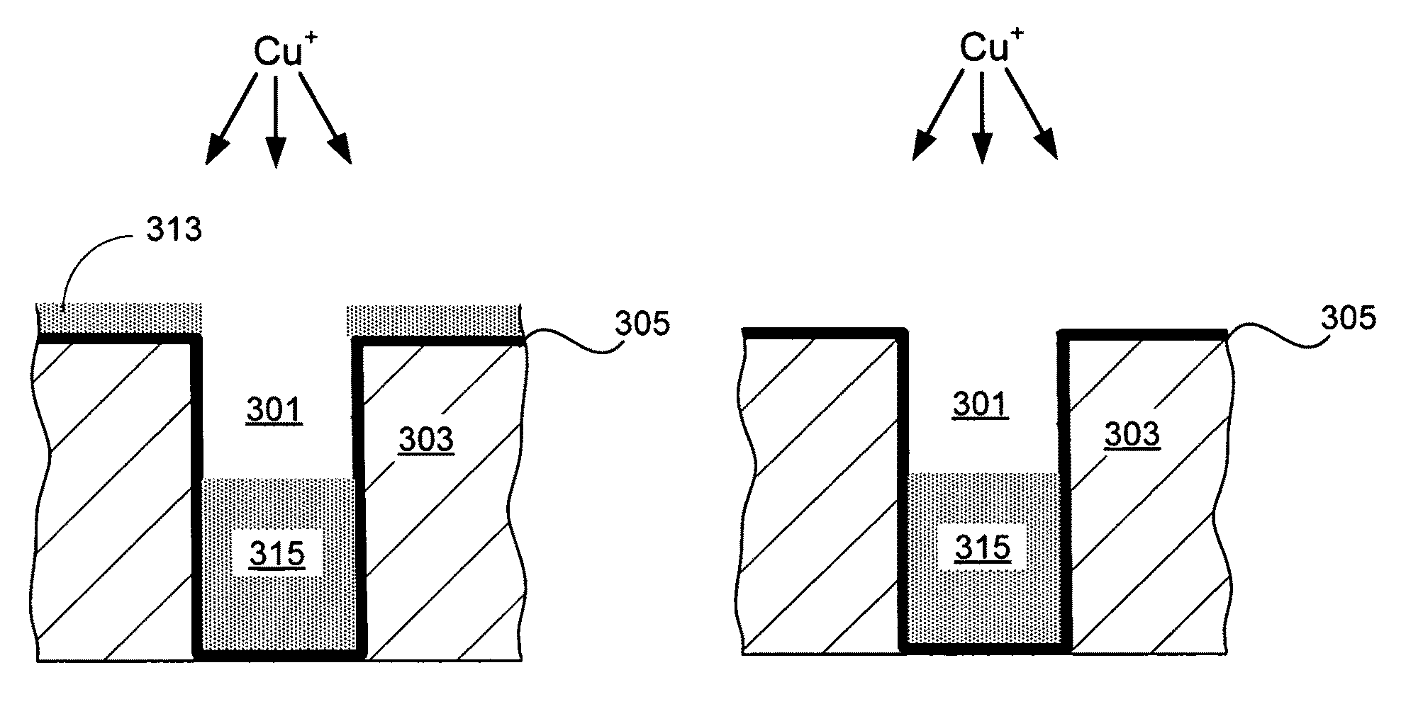
[0060]In the first embodiment, metal is deposited both within the recessed feature and on the field, such that the net deposition rate at the feature bottom is greater than the net deposition rate on the field. This embodiment is illustrated in FIG. 3A, where a cross-sectional depiction of a partially fabricated substrate undergoing deposition is shown. FIG. 3A shows a cross-sectional depiction of a trench 301 formed in a layer of dielectric 303 and lined with a layer of diffusion barrier material 305. A flux of copper consisting essentially of positively charged copper ions is being sputtered onto the substrate from a copper target. Unlike neutral copper atoms, ionized copper shows a more narrow angle distribution with a large fraction of ions arriving at a 90° angle to the wafer. This improves bottom coverage and reduces overhang. Further, copper ions have high mobility, and may migrate on the substrate surface until they arrive to the point of lowest energy, typically at the rece...

second embodiment

[0061]In the second embodiment, metal is deposited within the recessed feature while no net deposition or etching occurs in the field region. This is illustrated in FIG. 3B, where copper fill 315 resides within the trench, while no copper overburden is formed on the field region, and the diffusion barrier layer 203 remains exposed. In this case E / D ratio is less than 1 at the trench bottom, and is about 1 in the field region.

third embodiment

[0062]In the third embodiment, metal is deposited within the recessed feature while material is simultaneously removed (net etched) from the field region. This is illustrated in FIG. 3C, where the trench 301 is partially filled with copper layer 315, while diffusion barrier material is completely removed from the field exposing the dielectric layer 307. In this case E / D ratio is less than one at the trench bottom but is greater than one in the field region.

[0063]The net deposition rates of at least about 40 Å / second at the trench bottom can be achieved by this method. When etching of diffusion barrier material is occurring in the field simultaneously with recess fill, net etch rates of at least about 1 Å / second in the field can be achieved. For example a 400 nm deep trench can be filled in 100 seconds, while within the same time a 100 Å thick diffusion barrier material may be simultaneously removed from the field region.

[0064]It is understood that provided methods can be used to com...


PUM

PropertyMeasurementUnit
Fractionaaaaaaaaaa
Fractionaaaaaaaaaa
Fractionaaaaaaaaaa

Abstract

Recessed features on a Damascene substrate are filled with metal using plasma PVD. Recessed features having widths of less than about 300 nm, e.g., between about 30-300 nm can be filled with metals (e.g., copper and aluminum), without forming voids. In one approach, the deposition is performed by exposing the substrate to a high-density plasma characterized by high fractional ionization of metal. Under these conditions, the metal is deposited within the recess, without forming large overhang at the opening of the recess. In some embodiments, the metal is deposited within the recess, while diffusion barrier material is simultaneously etched from the field region. In a second approach, recessed features are filled by performing a plurality of profiling cycles, wherein each cycle includes a net etching and a net depositing operation. Etching and depositing parameters are adjusted such that the recessed features are filled without forming overhangs and voids.

Description

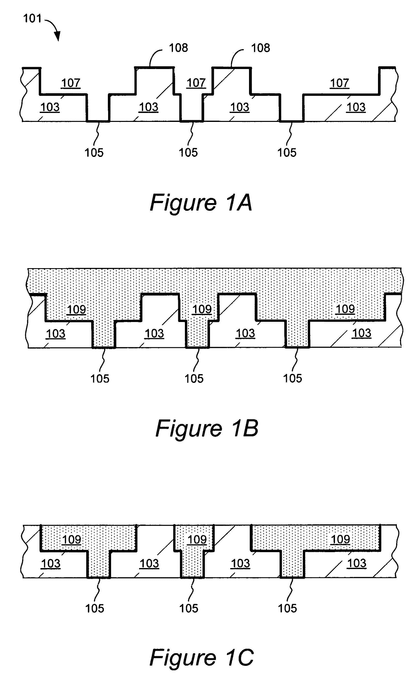
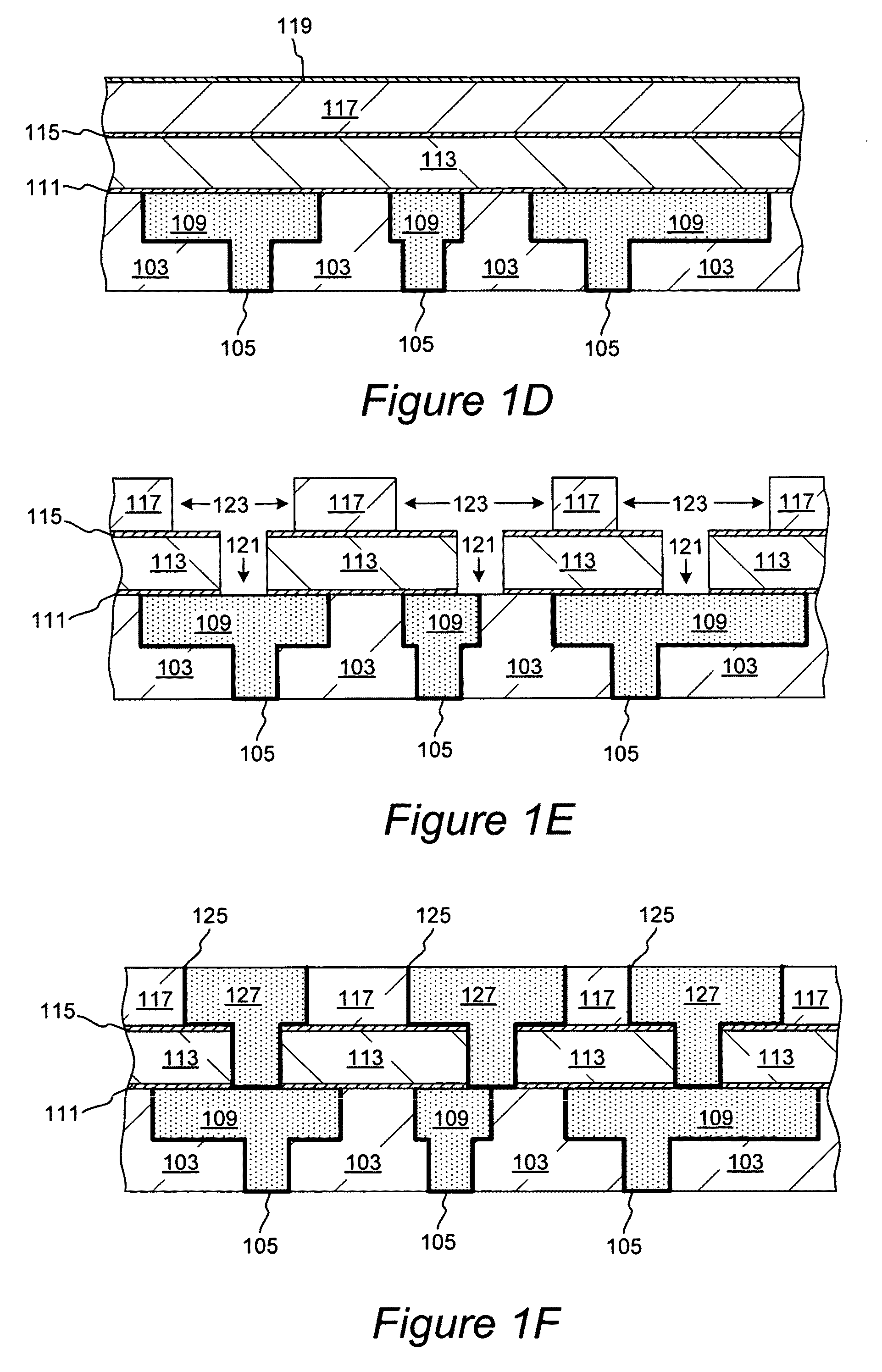
FIELD OF THE INVENTION[0001]The present invention pertains to methods of fabricating interconnections in semiconductor devices. The methods employ physical vapor deposition (PVD) for filling recessed features on partially fabricated semiconductor devices with metals. The methods are particularly useful for filling vias and trenches in a Damascene substrate with copper.BACKGROUND OF THE INVENTION[0002]Currently used integrated circuit (IC) fabrication methods commonly involve deposition of metals into recessed features formed in a layer of inter-layer dielectric (ILD). The deposited metal provides the conductive paths which extend horizontally and vertically within the IC substrate, connecting the active devices (e.g., transistors) in a desired pattern. The metal lines formed in adjacent ILD layers are connected to each other by a series of interconnections (interconnects). On a typical wafer substrate, one or several layers of dielectric are deposited onto a layer containing the act...

Claims


Application Information

Patent Timeline
IPC IPC(8): H01L21/44
CPCC23C14/046C23C14/165H01J37/3405H01L21/76883H01L21/76807H01L21/76877H01L21/76879H01L21/2855H01L21/76865
Inventor SHAVIV, ROEYDULKIN, ALEXANDERJULIANO, DANIELKINDER, RONALD
Owner NOVELLUS SYSTEMS
Learn More