Etchant composition, and method of fabricating metal pattern and thin film transistor array panel using the same
What is AI technical title?
AI technical title is built by Patsnap AI team. It summarizes the technical point description of the patent document.
a technology of thin film transistors and compositions, applied in the field of compositions and compositions, can solve the problems of stepping difference and other wiring lines placed over enlarged wiring lines, and achieve the effects of uniform etching characteristics, good etch profiles, and excellent productivity
Active Publication Date: 2011-06-28
SAMSUNG DISPLAY CO LTD +1
View PDF5 Cites 2 Cited by
Summary
Abstract
Description
Claims
Application Information
AI Technical Summary
This helps you quickly interpret patents by identifying the three key elements:
Problems solved by technology
Method used
Benefits of technology
Benefits of technology
The present invention provides an etchant composition and a method of fabricating a metal pattern and a thin film transistor array panel. The etchant composition includes a specific combination of phosphoric acid, nitric acid, and acetic acid, as well as a compound containing phosphate, a compound simultaneously containing an amino group and a carboxyl group, and an organic acid. The etchant composition has good etching characteristics of wiring lines and can be used for etching a single-layered structure based on copper or a copperalloy and a multi-layered structure of two or more layers based on the copper or copper alloy. The etchant composition may also include an etch control agent, a surfactant, a metalionsequestering agent, a corrosion inhibitor, and a pH control agent. The method of fabricating a thin film transistor array panel includes steps of forming gate lines and data lines on an insulation substrate, depositing a metal layer, and etching the metal layer using the etchant composition.
Problems solved by technology
However, certain difficulties may be encountered with the enlarged thickness thereof such that a stepped difference may be made due to the thickness enlargement and other wiring lines placed over the enlarged wiring lines may be broken due to the stepped difference.
Method used
Image
Click on the blue label to locate the original text in one second.
Reading with bidirectional positioning of images and text.
Examples
examples
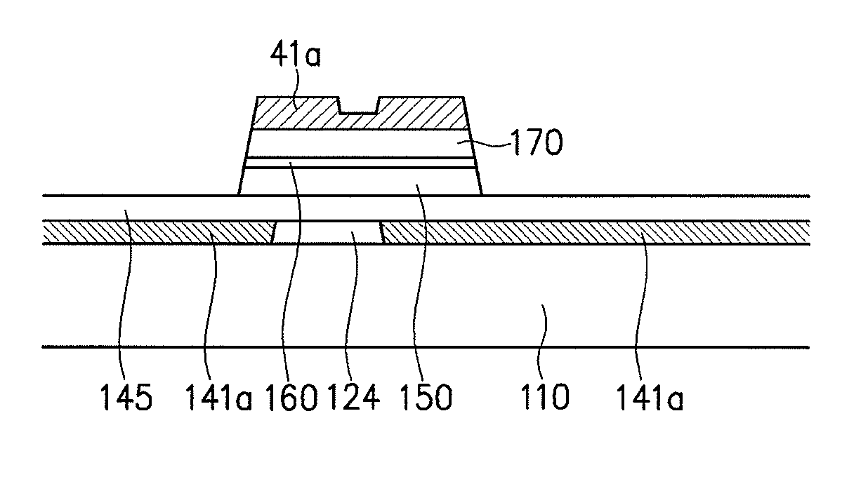
[0068]A display panel with metal wiring layers containing copper or a copper alloy was fabricated.
[0069]A substrate based on a glass material with a size of about 300× about 400 mm was prepared, and metal layers containing copper or a copper alloy were deposited onto the substrate as gate and data lines. A photoresist pattern was formed on the metal layers.
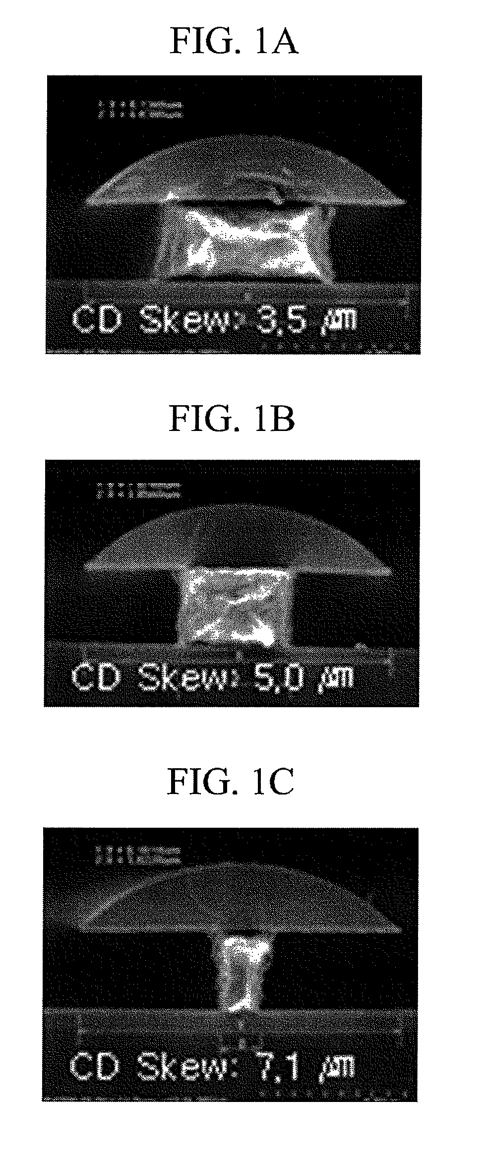
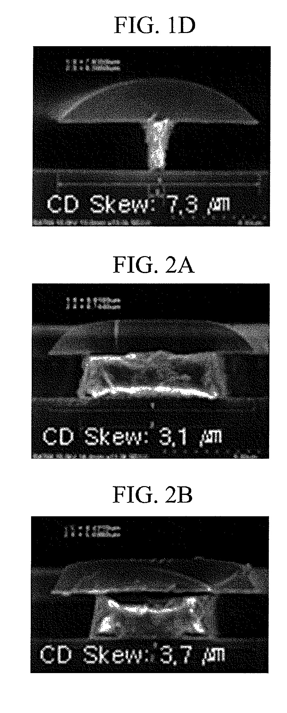
[0070]An etchant composition of about 180 kg containing phosphoric acid (H3PO4), nitric acid (HNO3), acetic acid (CH3COOH), glycolic acid, sodium dihydrogen phosphate, iminodiacetic acid, and water in accordance with the composition ratios listed in Table 1 was prepared. The etchant composition was put into experimental spray etching equipment (manufactured by K. C Tech Company, model ETCHER(TFT)), and the etching process was conducted at about 30° C., about 33° C., and about 35° C. The total etch time was established such that the time detected by an end point detector (EPD) was added by the amounts of about 50%, about 70%, about...
PUM
Property
Measurement
Unit
wt %
aaaaa
aaaaa
size
aaaaa
aaaaa
taper angle
aaaaa
aaaaa
Abstract
An etchant composition is provided. The etchant composition includes about 40 to about 65 wt % of phosphoric acid, about 2 to about 5 wt % of nitric acid, about 2 to about 20 wt % of acetic acid, about 0.1 to about 2 wt % of a compound containing phosphate, about 0.1 to about 2 wt % of a compound simultaneously containing an amino group and a carboxyl group, and a remaining weight percent of water for the total weight of the composition.
Description
CROSS-REFERENCE TO RELATED APPLICATION[0001]This application claims priority to Korean Patent Application No. 10-2008-0110435 filed on Nov. 7, 2008, the entire disclosure of which is hereby incorporated by reference herein in its entirety.BACKGROUND[0002](a) Technical Field[0003]The present disclosure relates to an etchant composition, and to a method of fabricating a metal pattern and a thin film transistor array panel.[0004](b) Description of the Related Art[0005]In recent times, there has been an increase in the amount of the usage of flat panel displays, such as, for example, a liquid crystal display, a plasmadisplay device, an electrophoretic display, and an organic electroluminescence device.[0006]Such a display device may be provided with a thin film transistor, which may be connected to gate and data lines crossing each other in an insulated manner.[0007]Scan signals (or gate signals), such as a gate-on voltage and a gate-off voltage, may be input through the gate line, and...
Claims
Application Information
Patent Timeline
Application Date:The date an application was filed.
Publication Date:The date a patent or application was officially published.
First Publication Date:The earliest publication date of a patent with the same application number.
Issue Date:Publication date of the patent grant document.
PCT Entry Date:The Entry date of PCT National Phase.
Estimated Expiry Date:The statutory expiry date of a patent right according to the Patent Law, and it is the longest term of protection that the patent right can achieve without the termination of the patent right due to other reasons(Term extension factor has been taken into account ).
Invalid Date:Actual expiry date is based on effective date or publication date of legal transaction data of invalid patent.

