Preparation of ultra-shallow semiconductor junctions using intermediate temperature ramp rates and solid interfaces for defect engineering

a semiconductor junction and intermediate temperature ramp technology, applied in semiconductor/solid-state device manufacturing, basic electric elements, electric apparatus, etc., can solve the problems of reducing the physical dimension of the dopant-containing layer, impede the feature size and spacing requirements of electrical components in dense integrated electrical circuits, and no known manufacturing solution to meet the requirements of rapidly evolving device requirements

Active Publication Date: 2011-06-28
THE BOARD OF TRUSTEES OF THE UNIV OF ILLINOIS
View PDF34 Cites 96 Cited by
  • Summary
  • Abstract
  • Description
  • Claims
  • Application Information

AI Technical Summary

Benefits of technology

[0021]In another embodiment, treatment with a surface modification agent results in at least a portion of the semiconductor surface having dangling bonds. Other methods aside from treatment with a surface modification agent may also be used for generation of an atomically clean or undersaturated semiconductor surface or a semiconductor surface having dangling bonds. For specific embodiments, the treatment with a surface modification agent occurs before any step annealing the semiconductor having implanted dopants. For some of these embodiments, the treatment step allows for control over the rates and extent of dopant diffusion during a subsequent annealing step.
[0022]Surface modifying agents useful in the methods described herein are also capable of interacting with semiconductor surfaces in a manner generating diffusion control groups or surface modification groups on an exposed semiconductor surface, preferably a selected surface abundance or population of diffusion control groups on an exposed semiconductor surface. Diffusion control groups can selectively increase or decrease the loss rate of semiconductor interstitial with the semiconductor surface. For some embodiments, the surface abundance of diffusion control groups is controlled by selection of the composition of one or more of the surface modifying agents exposed to the semiconductor surface, the exposure time, the temperature of the semiconductor surface during exposure, concentrations or partial pressures of one or more surface modifying agents exposed to the semiconductor surface, the total pressure of the system during exposure or any combination of these parameters. In one embodiment, the surface abundance of diffusion control groups is selected from the range of about 1×10¹² molecules cm−2 to about 2×10¹⁵ molecules cm−2, more preferably for some applications 4×10¹⁴ molecules cm−2 to about 9×10¹⁴ molecules cm−2. Alternatively, the surface abundance of diffusion control groups is selected from the range of about 0 to about 3 monolayers, and more preferably for some applications 0.001 monolayers to about 1.5 monolayers. U.S. patent application Ser. No. 11 / 192,339 (U.S. Patent Application Publication No. 2006 / 0024928), the disclosure of which is herein incorporated by reference in its entirety, discloses methods of treating a semiconductor with surface modification agents for control of dopant diffusion and activation. In specific embodiments, the amount and / or surface abundance of diffusion control groups present on the surface allows for selection and / or control of the surface annihilation probability for interstitial atoms, the interface annihilation probability for interstitial atoms. In embodiments, the amount and / or surface abundance of diffusion control groups present on the surface allows for selection and / or control over the rates and / or extents of dopant diffusion which occur during annealing, thereby achieving a selected dopant profile.

Problems solved by technology

The International Technology Roadmap for Semiconductors currently acknowledges, however, that there are no known manufacturing solutions to satisfy these rapidly evolving device requirements.
Accordingly, fabrication of extremely shallow dopant-containing semiconductor layers having low electrical resistance, such as dopant-containing layers comprising P-N junctions in CMOS transistors, is a fundamental barrier to continued advances in the performance of many microelectronic devices.
Furthermore, thermal diffusion methods are susceptible to problems associated with lateral diffusion of dopants, poor control of dopant concentrations and a propensity to generate dislocations, which can significantly impede satisfaction of the feature size and spacing requirements of electrical components in dense integrated electrical circuits.
Subsequent annealing of the dopant-containing layer, however, inevitably causes dopant atoms to diffuse, which thereby increases the physical dimensions of the dopant-containing layer.
Current annealing technologies have run into a limit in their ability to simultaneously increase dopant activation and decrease dopant diffusion, especially for the key dopant boron.
This problem has been worsened by the need to continually reduce processing temperatures to avoid damaging structures already in place during device fabrication.
Both flash and laser annealing can be employed in various combinations with spike annealing, mainly because it is found empirically that the millisecond techniques do a comparatively poor job of removing implantation damage, which leads to harmful leakage currents in the final device.
Up to now there has been little rational design for these recipes because the mechanisms by which millisecond annealing techniques achieve their improvements in dopant activation and diffusion (compared to spike annealing) were unknown.
There have also been problems with metastability of the activated dopant in millisecond annealing; subsequent thermal steps tend to decrease the degree of dopant activation.
These complex diffusion mechanisms constitute a fundamental limit on the control of physical dimensions of dopant-containing layers prepared by ion implantation methods and currently impede reproducible fabrication of ultra-shallow (<200 nm) dopant-containing layers.
The undesirable effects of TED are exacerbated by the higher concentrations of active dopant required for improved microelectronic device performance.
Such high concentrations are well above the thermodynamic solubility limit and, thus the corresponding structures are thermodynamically unstable.
Ion implantation at the high ion fluxes required to achieve such dopant concentrations creates a large number of defects and interstitials in the bulk phase of the semiconductor substrate which promotes fast TED of the dopants during annealing.
These TED mechanisms involving interstitials ultimately results in significant junction deepening.
In addition, implantation at high ion fluxes may generate electrically charged defect sites residing at the exposed surface of the semiconductor layer in sufficient numbers that they couple to the motion of charge defects in the underlying bulk.
Such defect engineering methods, however, have generally demonstrated limited utility.
While these methods may effectively limit the occurrence of TED, implementation of these methods is expected to require solutions to a large number of problems associated with integration of these methods into existing and well developed semiconductor processing techniques.
Such integration issues remain a significant barrier to adoption of these approaches for fabricating ultra-shallow dopant-containing semiconductor layers.

Method used


Image

  • Preparation of ultra-shallow semiconductor junctions using intermediate temperature ramp rates and solid interfaces for defect engineering
  • Preparation of ultra-shallow semiconductor junctions using intermediate temperature ramp rates and solid interfaces for defect engineering
  • Preparation of ultra-shallow semiconductor junctions using intermediate temperature ramp rates and solid interfaces for defect engineering

Examples


example 1

Optimized Temperature Ramp Rates

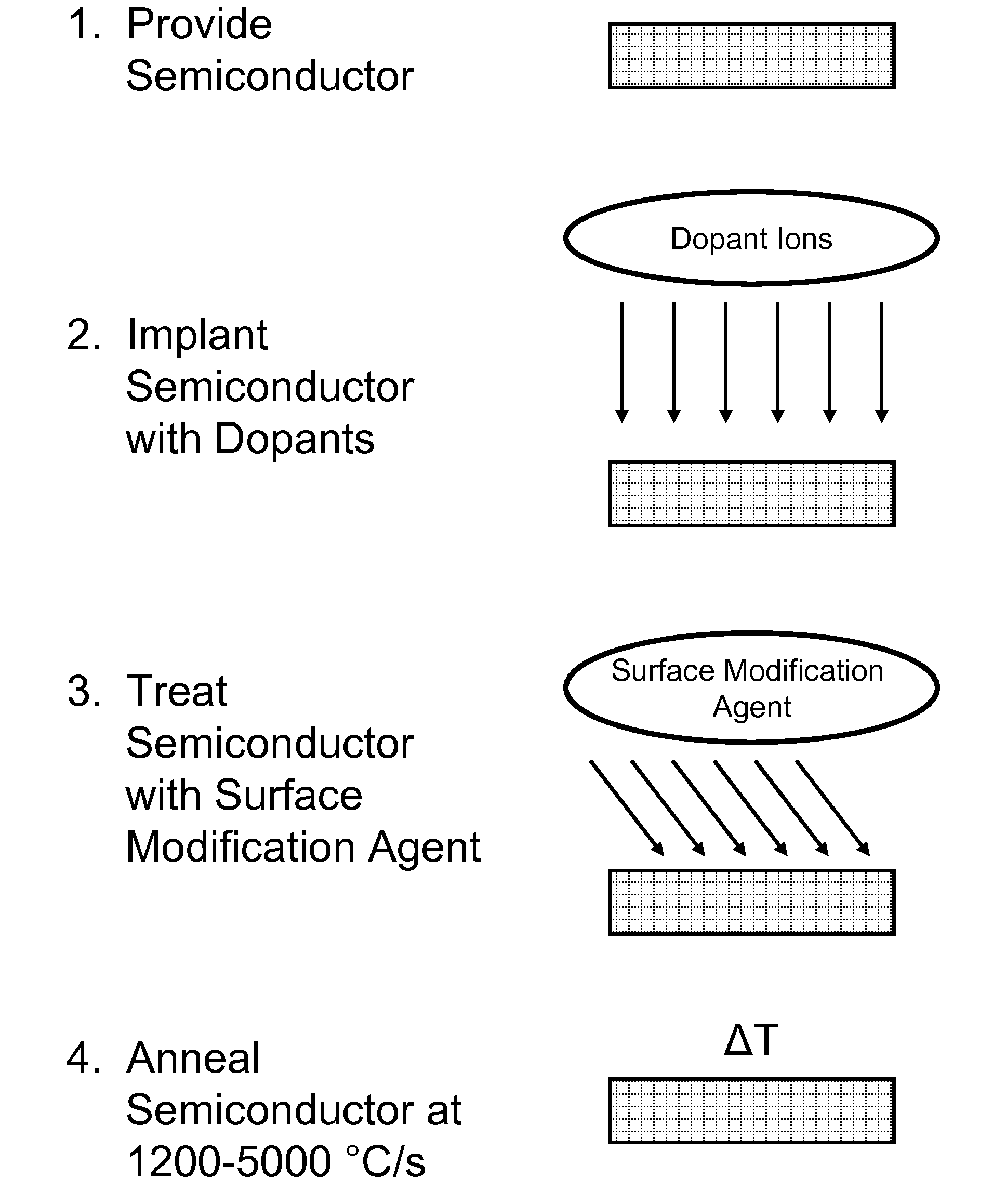
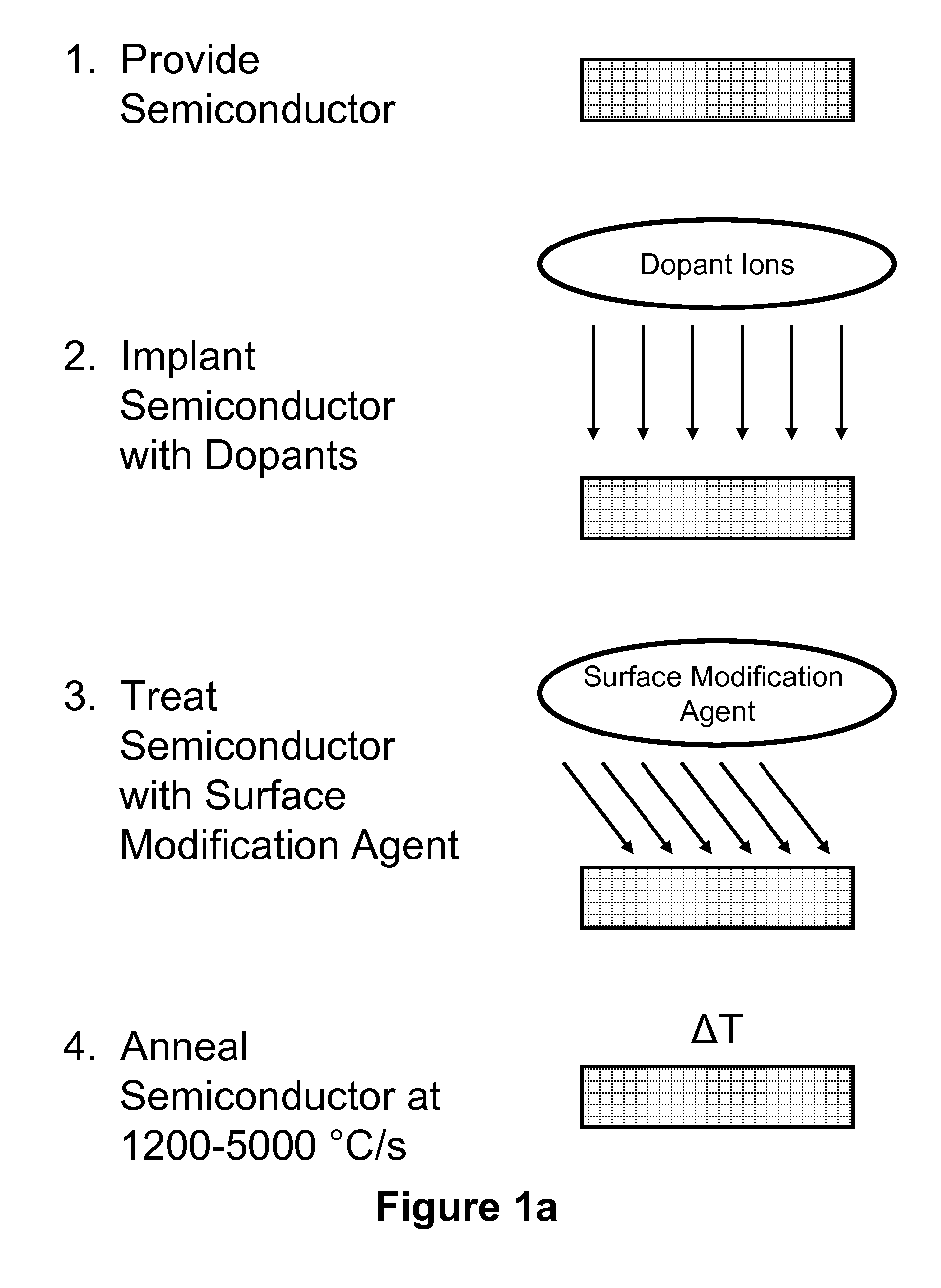
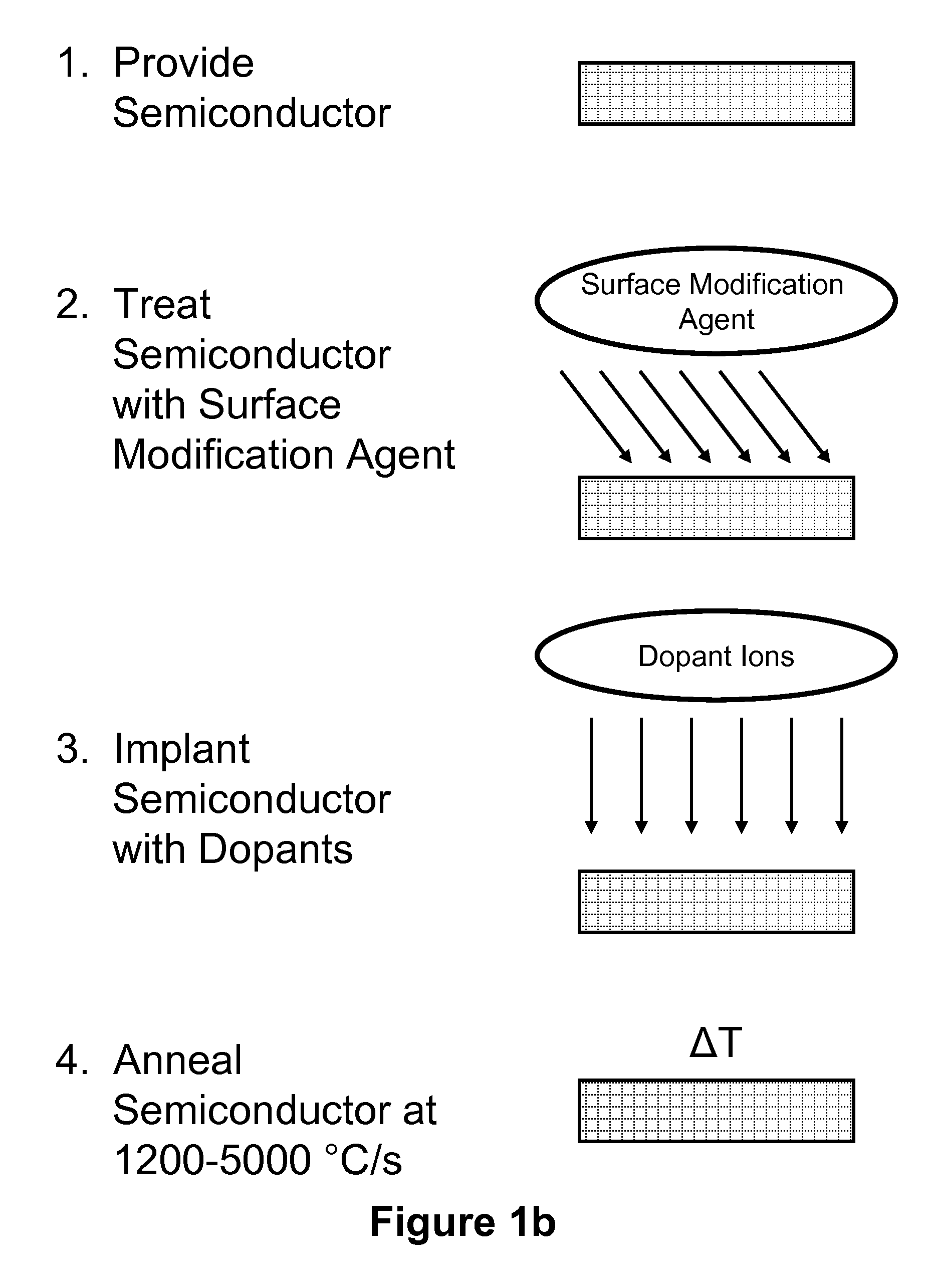
[0068]Background. In “soak” annealing, a semiconductor wafer is held at constant temperature for several minutes. It is sometimes used for “solid phase epitaxial regrowth” (SPER), in which a doped layer of amorphous silicon is grown and then heated with the huge crystalline seed layer underneath to guide the crystal formation of the doped layer. Much research has gone into SPER, though it does not appear to be the method the semiconductor industry is moving toward.

[0069]In “spike” annealing, the temperature is ramped by incandescent light heating (after a temperature stabilization step of several tens of seconds at 600-800° C.) at 25-400° C. / second up to typically about 1050° C. The dwell time near the top of the spike is 0.5-1 second, and is governed by the time it takes for lamps to cool down after power is cut.

[0070]There are two kinds of millisecond heating methods that the industry is moving toward. One is “flash” annealing, wherein the wafer is ...

example 2

Use of Solid Interfaces for Defect Engineering

[0096]Introduction. A substantial difference in diffusion profiles of arsenic implanted into silicon is observed when soak annealing is performed in the presence of a silicon dioxide overlayer grown at 630° C. vs. a native oxide grown at room temperature by simple exposure to air. Substantial differences in arsenic activation as measured by sheet resistance are also observed. Similar effects are observed for the fraction of arsenic dose retained.

[0097]In these cases, the oxide was formed before annealing took place. It is also possible to form or grow the oxide during the annealing step employed for activating the dopant. Varying the ambient gas pressure of oxygen results in significantly different degrees of boron diffusion, dose loss and fractional activation. In all cases, the results involved soak annealing and low pressures of oxygen: below 10−6 Torr. These low pressures would be difficult, though not impossible (with effort) to ach...

example 3

Simulation Results

[0112]Simulations conducted illustrate that flash annealing is an improvement over spike. As shown in Table 4, a 20 times increase in Si interstitial concentration (from 4×10¹⁴ to 9×1015 cm−3) is more than counterbalanced by the factor of 1000 decrease in time the profiles are exposed to these concentrations, resulting in an improvement in junction depth. FIGS. 5A and 5B show several examples of results distilled from the simulations according to the criteria shown above in Example 1.

[0113]

TABLE 4Spike (1050° C.)Flash (1322° C.)[Sii] (cm−3)4 × 10149 × 1015tmax (S)0.66 × 10⁻⁴xlattice (nm)22.74.8x (expt) (nm)21.54.7

[0114]FIGS. 9A and 9B illustrate two mechanisms by which boron is immobilized. In the first mechanism, FIG. 9A, a boron interstitial 901 is immobilized by kick-in into the semiconductor 902 lattice. In the second mechanism, FIG. 9B, a boron interstitial 903 is accreted into a boron 904 and semiconductor 905 cluster. FIG. 7 shows a cartoon representation of...


PUM

PropertyMeasurementUnit
temperatureaaaaaaaaaa

Abstract

Described herein are processing conditions, techniques, and methods for preparation of ultra-shallow semiconductor junctions. Methods described herein utilize semiconductor surface processing or modification to limit the extent of dopant diffusion under annealing conditions (e.g. temperature ramp rates between 100 and 5000° C. / second) previously thought impractical for the preparation of ultra-shallow semiconductor junctions. Also described herein are techniques for preparation of ultra-shallow semiconductor junctions utilizing the presence of a solid interface for control of dopant diffusion and activation.

Description

CROSS REFERENCE TO RELATED APPLICATION[0001]This application claims priority under 35 U.S.C. §119(e) to U.S. Provisional Patent Application No. 61 / 037,882 filed on Mar. 19, 2008, which is hereby incorporated by reference in its entirety.BACKGROUND OF THE INVENTION[0002]This invention is in the field of semiconductor processing. This invention relates generally to techniques for preparation of ultra-shallow semiconductor junctions.[0003]The continuing trend toward smaller, higher speed microelectronic devices requires integrated circuit designs characterized by smaller feature sizes and closer spacing between electrical components. These requirements have generated an immediate demand for methods for fabricating extremely shallow and spatially well defined dopant-containing semiconductor layers that exhibit very low electrical resistance in microelectronic devices. For example, current complementary metal oxide semiconductor (CMOS) transistors in integrated microelectronic circuits r...

Claims


Application Information

Patent Timeline
Patent Type & Authority Patents(United States)
IPC IPC(8): H01L21/425H01L21/265
CPCH01L21/26513H01L21/324H01L21/2652H01L21/26566
Inventor SEEBAUER, EDMUND G.
Owner THE BOARD OF TRUSTEES OF THE UNIV OF ILLINOIS
Why Eureka
Try Eureka