
Self auto-calibration of analog circuits in a mixed signal integrated circuit device

a mixed signal integrated circuit and self-auto-calibration technology, applied in the direction of low noise amplifiers, instruments, code conversion, etc., can solve the problems of inefficient on-line calibration of analog functions and expensive equipment used to test the functions of digital microcontrollers, and achieve the effect of minimizing the input offset voltage of the analog input devi

Active Publication Date: 2011-07-05
MICROCHIP TECH INC
View PDF6 Cites 21 Cited by
  • Summary
  • Abstract
  • Description
  • Claims
  • Application Information

AI Technical Summary

Benefits of technology

In addition, a user may compensate for variations in the end system, including operating point, e.g., power supply, common-mode, etc.; environmental changes, e.g., temperature, humidity, etc.; and also to compensate for component drift over time, e.g., aging effects, etc.
The analog input device has input offset voltage compensation or a trimming circuit that counteracts or compensates for the device input offset voltage by applying, for example, but not limited to, an opposite polarity voltage between the differential inputs of the analog input device so as to minimize the resulting voltage error at the output of the analog device. Switching of resistances, current sources and / or voltage sources in the differential input circuit of the analog input device may be used to compensate for the input offset voltage error. In addition, a digital-to-analog converter (DAC) may be used to generate a compensation voltage to overcome the input offset voltage error. It is contemplated and within the scope of this disclosure that other ways of compensating for the input offset voltage error may be utilized so long as they can be controlled by applying a digital value thereto.
The input offset voltage compensation circuit of the analog input device may have a storage register or memory that retains the digital value required for compensating the input offset voltage. This storage register may be volatile or nonvolatile depending upon the application desired. Therefore, no factory calibration during manufacture and / or testing is required, programmable fuse link trimming may be eliminated, and end user application flexibility increased.
A plurality of analog input devices may have their input offset voltages compensated for by multiplexing the digital control circuit and comparator between each of the plurality of analog input devices. Thus circuits and die area are reduced, saving costs and improving reliability of a mixed-signal integrated circuit device.
According to another specific example embodiment of this disclosure, a method for minimizing an input offset voltage in an analog input device upon an occurrence of an event, comprises the steps of: (a) detecting an occurrence of an event; (b) switching from a normal mode to an auto-calibration mode upon detection of the occurrence of the event an analog input device having an input offset voltage compensation circuit; (c) applying a reference voltage to the analog input device; (d) minimizing an input offset voltage of the analog input device by: (i) measuring an output voltage of the analog input device; and (ii) applying input offset compensation values to the input offset voltage compensation circuit until the output voltage from the analog input device is at a desired value and then storing the input offset compensation value that minimizes the input offset voltage of the analog input device; and (e) switching the analog input device from the calibration mode to the normal mode.

Problems solved by technology

This calibration step takes time during manufacturing / testing of the op-amp, and is therefore generally expensive to perform.
This creates an additional problem in that the equipment used to test the digital microcontroller functions is not capable of performing on-line calibration of analog functions efficiently.

Method used


Image

  • Self auto-calibration of analog circuits in a mixed signal integrated circuit device
  • Self auto-calibration of analog circuits in a mixed signal integrated circuit device
  • Self auto-calibration of analog circuits in a mixed signal integrated circuit device

Examples


Embodiment Construction

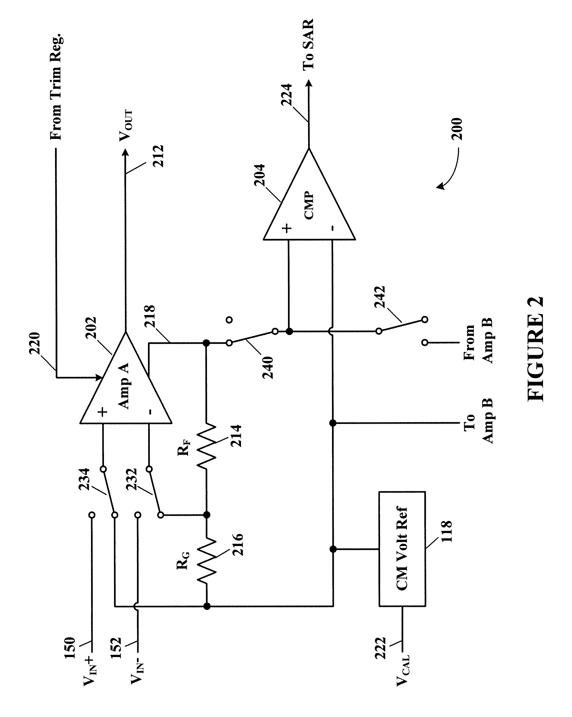
Referring now to the drawings, the details of example embodiments are schematically illustrated. Like elements in the drawings will be represented by like numbers, and similar elements will be represented by like numbers with a different lower case letter suffix.

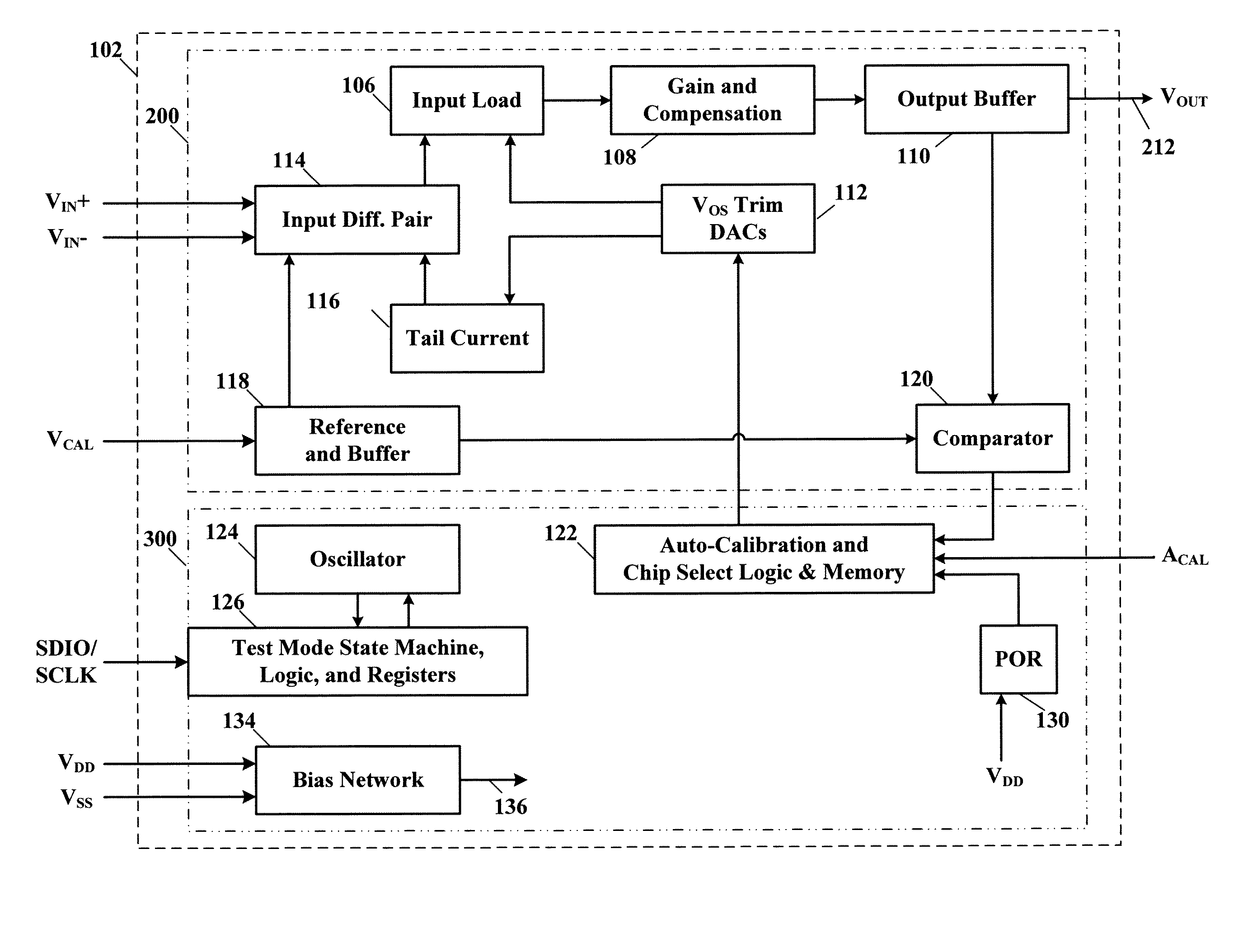
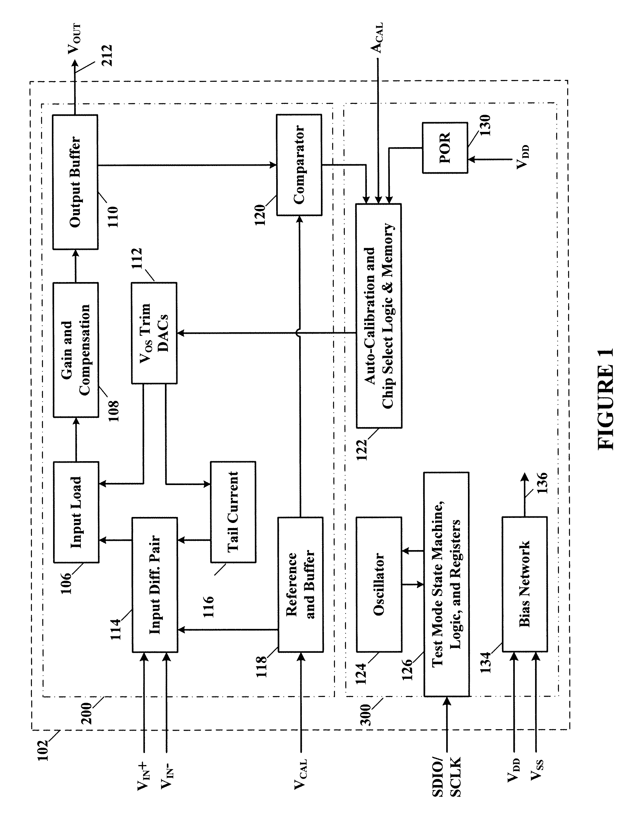
Referring to FIG. 1, depicted is a schematic block diagram of a self auto-calibration device for a differential input operational amplifier, according to a specific example embodiment of this disclosure. The self auto-calibration device 102 comprises an analog portion 200 (see FIG. 2) and a digital portion 300 (see FIG. 3). The analog portion 200 comprises an input differential pair 114, a gain and compensation circuit 108 and an output buffer 110 of a differential input operational amplifier, voltage offset compensation digital-to analog-converters (DACs) 112, an input load 106, a tail current circuit 116, a calibration voltage reference and buffer 118, and a voltage comparator 120. The digital calibration portion 300 compr...


PUM


Abstract

Auto-calibration of the analog circuits occurs when requested by a user and / or the occurrence of an event(s). The user may invoke an auto-calibration on demand through an auto-calibration (ACAL) input to the mixed-signal integrated circuit. An external voltage calibration (VCAL) input may be used for auto-calibration of the mixed-signal integrated circuit to a user-supplied common-mode voltage reference. Auto-calibration of the mixed-signal integrated circuit may also be initiated upon the occurrence of any one or more of the following events: 1) detection of auto-calibration data corruption, e.g., parity checking of auto-calibration data values digitally stored in the mixed-signal integrated circuit; 2) an internal timer that causes a calibration request after a programmable timeout period, 3) change in the internal integrated circuit die temperature as determined by a temperature sensor, and 4) a change in the power supply and / or internal supply voltage(s).

Description

TECHNICAL FIELDThe present disclosure relates to integrated circuits having analog input devices and, more particularly, to an auto-calibration circuit for minimizing input offset voltage in the integrated circuit analog input device.BACKGROUNDIntegrated circuits are becoming far more sophisticated while continuing to drop in price. Combinations of both analog and digital functions fabricated on an integrated circuit die, or packaged in a multi-chip package (MCP), are becoming more prevalent and are further increasing the usefulness and reducing the cost of consumer and industrial products. The combination of a microcontroller, and analog and digital circuit functions on an integrated circuit die or in an MCP has also expanded the useful range of applications. Consumer and commercial products, such as, for example, but not limited to, appliances, telecommunications devices, automobiles, security systems, full-house instant hot water heaters, thermostats and the like, are being contr...

Claims


Application Information

Patent Timeline
IPC IPC(8): H03M1/06
CPCH03F3/195H03F3/45475H03F3/45977H03M1/1009H03F2200/261H03F2200/294H03F2200/451H03F2203/45048H03F2203/45136H03M1/12
Inventor NOLAN, JAMES B.BLAKE, KUMEN
Owner MICROCHIP TECH INC
Learn More