Thermal processing apparatus

a technology of thermal processing apparatus and thermal processing apparatus, which is applied in the direction of lighting and heating apparatus, ovens, ovens, etc., can solve the problems of insufficient annealing process of a higher temperature, the provision of such bulky shutting mechanism, and the structure of the thermal processing apparatus, so as to improve the heating efficiency of the object, the effect of rapid increase and decrease of the temperature of the obj

Inactive Publication Date: 2011-07-12
TOKYO ELECTRON LTD
View PDF19 Cites 9 Cited by
  • Summary
  • Abstract
  • Description
  • Claims
  • Application Information

AI Technical Summary

Benefits of technology

[0007]Taking account of the above problems, the present invention has been made to efficiently cope therewith. An objective of the present invention is to provide a thermal processing apparatus capable of rapidly increasing and decreasing a temperature of an object to be processed, when the object is subjected to a thermal process at a high temperature. Another objective of the present invention is to provide a thermal processing apparatus capable of improving a heating efficiency of the object.
[0018]This structure allows a rapid lowering of the temperature of the object, while maintaining an intra-surface uniformity in the temperature of the object.
[0021]Due to this structure, an absorptance of the object with respect to the heat rays from the heating lamps is elevated, so that the temperature of the object can be more rapidly raised.
[0029]As stated above, the heating efficiency of the object disposed on the table can be further improved by the absorbing plate that mainly absorb the heat rays of a kind mainly irradiated from the heating lamps.

Problems solved by technology

Although the annealing process of the channel layer for a long period of time can stabilize the atomic structure, the long annealing process undesirably causes the impurity atoms to diffuse downward in a film-thickness direction of the channel layer to penetrate the same.
However, the conventional thermal processing apparatus having the shutting mechanism is disadvantageous in that a bulk of the shutting mechanism enlarges the size of the thermal processing apparatus, and a provision of such bulky shutting mechanism complicates a structure of the thermal processing apparatus.
On the other hand, the conventional thermal processing apparatus having the Peltier element is suitable for the etching process using a process temperature as low as 100° C. to 250° C., but the apparatus is insufficient to perform the annealing process of a higher temperature.

Method used


Image

  • Thermal processing apparatus
  • Thermal processing apparatus
  • Thermal processing apparatus

Examples


first embodiment

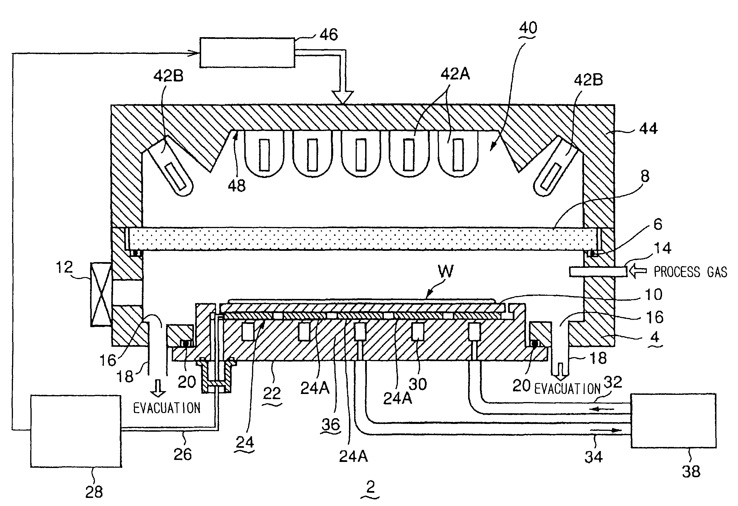
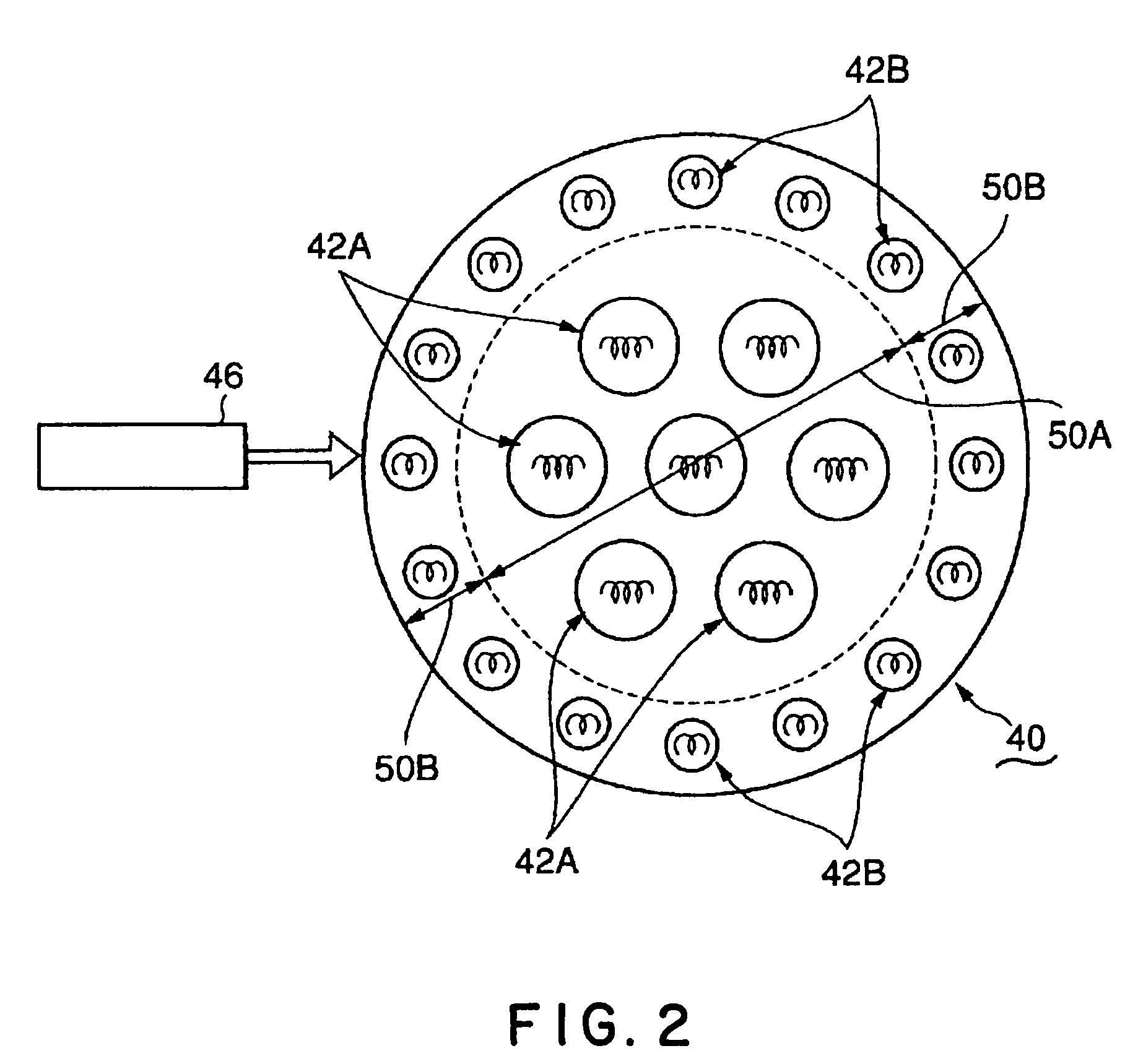
[0045]As shown in FIG. 1, a thermal processing apparatus 2 in a first embodiment of the present invention includes a cylindrical processing vessel 4 made of, e.g., aluminum. A top part of the processing vessel 4 is opened, and a transparent transmitting window 8 is air-tightly fitted in the top opening through a sealing member 6 such as an O-ring. A thin disk-shaped table 10 is disposed in the processing vessel 4. An object to be processed such as a semiconductor wafer W is supported on an upper surface of the table 10. The table 10 is formed of such a material that is best suited for absorbing a light ray irradiated from a heat lamp to be used. For example, the table 10 is formed of an SiO2 material, an AlN material, or an SiC material, which tends to mainly absorb a light ray from an infrared lamp. Alternatively, the table 10 is formed of a Ge (germanium) material, an Si material, or a metal material, which tends to mainly absorb a light ray from an ultraviolet lamp or a halogen l...

second embodiment

[0073]In the first embodiment, the table 10 is formed of a single material, but the present invention is not limited thereto. For example, the table 10 may be formed by stacking a plurality of absorbing plates having different main absorption wavelength bands.

[0074]FIG. 10 shows schematic views (A) and (B) of structures of a table in a second embodiment of the present invention. Illustration of structures other than the table 10 are omitted. Specifically, the table 10 is manufactured by stacking a visible-ray absorbing plate 62 that mainly absorbs the ultraviolet ray and the visible ray, and an infrared-ray absorbing plate 64 that mainly absorbs the infrared ray.

[0075]Regarding materials constituting the respective absorbing plates 62 and 64, the ultraviolet and visible-ray absorbing plate 62 may be a germanium plate or a silicon plate, for example, while the infrared-light absorbing plate 64 may be a quartz plate, an AlN plate, or an SiC plate, which has been as stated above referr...

third embodiment

[0079]Next, a third embodiment of the present invention is described below. FIG. 11 is a schematic sectional view of the third embodiment of the present invention. The same parts as those of FIG. 1 are depicted by the same reference numbers, and their description is omitted. As shown in FIG. 11, a reflecting plate 70 made of aluminum plating is disposed to cover all the upper surface of a heat-medium jacket 36 serving as a base plate 22 of a processing vessel 4. A table 10 is disposed on the reflecting plate 70 through Peltier elements 24A.

[0080]In the third embodiment, a heat ray that has transmitted a wafer W and the table 10 is reflected upward by the reflecting plate 70, and thus the heat ray again contributes to heating of the wafer W. Since the heating efficiency can be improved because of the reflected ray, the wafer can be more rapidly heated. It goes without saying that the structures of the second embodiment shown in FIG. 10(A) and FIG. 10(B) can be applied to the table 10...


PUM

PropertyMeasurementUnit
temperatureaaaaaaaaaa

Abstract

The present invention provides a thermal processing apparatus that conducts a thermal process such as an annealing process at a temperature of 400° C. or more to an object to be processed. The apparatus is provided with a processing vessel (4) having a transmitting window (8) in a top part thereof. A table (10) is disposed in the vessel, that supports thereon the object (W) opposed to the transmitting window. A plurality of heating lamps (42A, 42B) are disposed above the processing vessel, that heat the object by irradiating heat rays to the object through the transmitting window. A thermoelectric converter (24) is disposed on the table and configured to at least cool the object. When a temperature of the object is increased, the object is mainly heated by the heat rays from the heating lamps. When the temperature of the object is decreased, the object is forcibly cooled by means of the thermoelectric converter.

Description

TECHNICAL FIELD[0001]The present invention relates to a thermal processing apparatus that conducts thermal processes, such as an annealing process and a film-deposition process, to an object to be processed, e.g., a semiconductor wafer.BACKGROUND ART[0002]When a semiconductor device is manufactured, a semiconductor wafer is generally, repeatedly subjected to various thermal processes such as a film-deposition process, pattern-etching process, oxidation and diffusion process, modification process, annealing process, and so on, so as to manufacture a desired device. In the light of the recent demand for higher density, the increased number of layers, and higher integration of the semiconductor device, the semiconductor device should have strict specifications. In particular, an improvement in a wafer intra-surface uniformity and an improvement in a film quality are desired in the various thermal processes. For example, in a process of a channel layer of a transistor as a semiconductor...

Claims


Application Information

Patent Timeline
Patent Type & Authority Patents(United States)
IPC IPC(8): F26B3/30A21B1/22C23C16/00H01L21/31H01L21/00H01L21/26H01L21/324H01L35/28H01L35/30
CPCH01L21/324H01L21/67109H01L21/67115H01L21/26
Inventor SHIMIZU, MASAHIROKASAI, SHIGERUYONEDA, MASATAKE
Owner TOKYO ELECTRON LTD
Why Eureka
Try Eureka