Display device

a display device and display technology, applied in the field of display devices, can solve the problems of not always suitable for a larger glass substrate, and achieve the effects of reducing the area occupied by the connection portion, reducing the contact resistance, and reducing the size of the display devi

Active Publication Date: 2011-08-02
SEMICON ENERGY LAB CO LTD
View PDF164 Cites 64 Cited by
  • Summary
  • Abstract
  • Description
  • Claims
  • Application Information

AI Technical Summary

Benefits of technology

[0004]A thin film transistor in which a channel formation region is formed using an oxide semiconductor has properties as follows: the operation speed is higher than that of a thin film transistor including amorphous silicon and the manufacturing process is simpler than that of a thin film transistor including polycrystalline silicon. That is, the use of an oxide semiconductor makes it possible to manufacture a thin film transistor with high field effect mobility even at low process temperatures ranging from room temperature to 300° C. or lower.
[0007]Another object of the present invention is to enhance the function of a protective circuit and stabilize the operation in a display device intended for a variety of purposes manufactured by stacking an insulating film and a conductive film in addition to an oxide semiconductor.
[0014]In the non-linear element included in the protective circuit according to an embodiment of the present invention, the conductive layer of the first or second wiring layer is directly connected to the gate electrode or the wiring formed with the same layer as the gate electrode; thus, only one interface and one contact hole are formed for one connection. The connection method of the present invention enables contact resistance to be reduced as compared with the connection method using another wiring layer because the number of interfaces formed for one connection is only one. Accordingly, the protective circuit including the non-linear element operates stably. In addition, the connection method of the present invention enables an area occupied by the connection portion to be reduced as compared with the connection method using another wiring because only one contact hole is needed for one connection. Accordingly, an area occupied by the protective circuit can be reduced and reduction in size of the display device can be achieved.

Problems solved by technology

On the other hand, thin film transistors manufactured using polycrystalline silicon have high field effect mobility, but a crystallization step such as laser annealing is necessary and are not always suitable for a larger glass substrate.

Method used


Image

  • Display device
  • Display device
  • Display device

Examples


embodiment 1

[0042]In this embodiment, an example of a display device including a pixel portion and a protective circuit which includes a non-linear element provided near the pixel portion is described with reference to drawings.

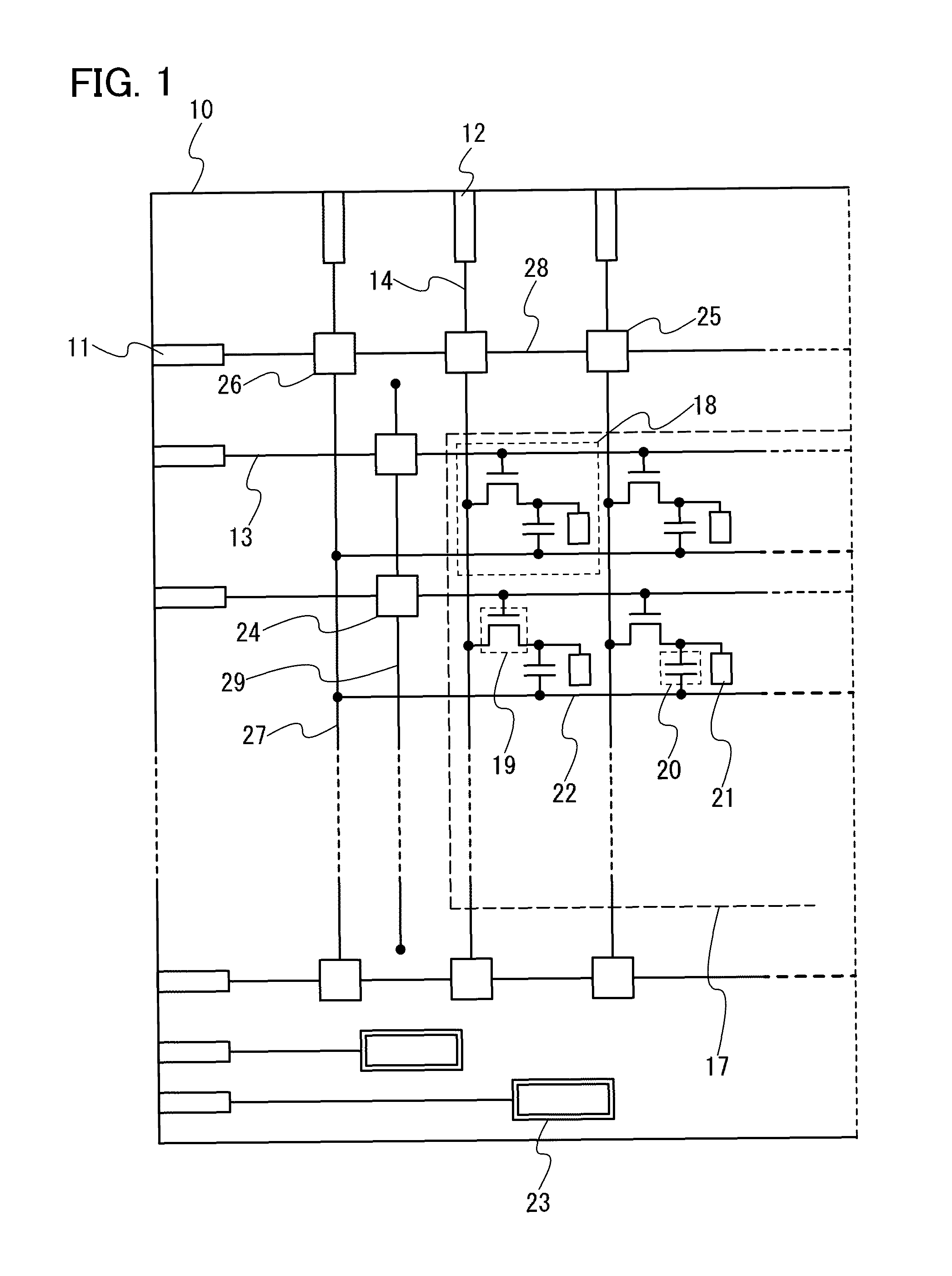
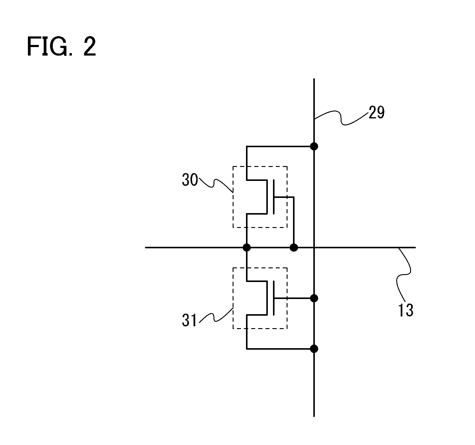
[0043]FIG. 1 illustrates a positional relationship among signal input terminals, scan lines, signal lines, protective circuits including non-linear elements, and a pixel portion in a display device. Over a substrate 10 having an insulating surface, scan lines 13 and signal lines 14 intersect with each other to form a pixel portion 17.

[0044]The pixel portion 17 includes a plurality of pixels 18 arranged in matrix. The pixel 18 includes a pixel transistor 19 connected to the scan line 13 and the signal line 14, a storage capacitor portion 20, and a pixel electrode 21.

[0045]In the pixel structure illustrated here, one electrode of the storage capacitor portion 20 is connected to the pixel transistor 19 and the other electrode is connected to a capacitor line 22. Moreover, t...

embodiment 2

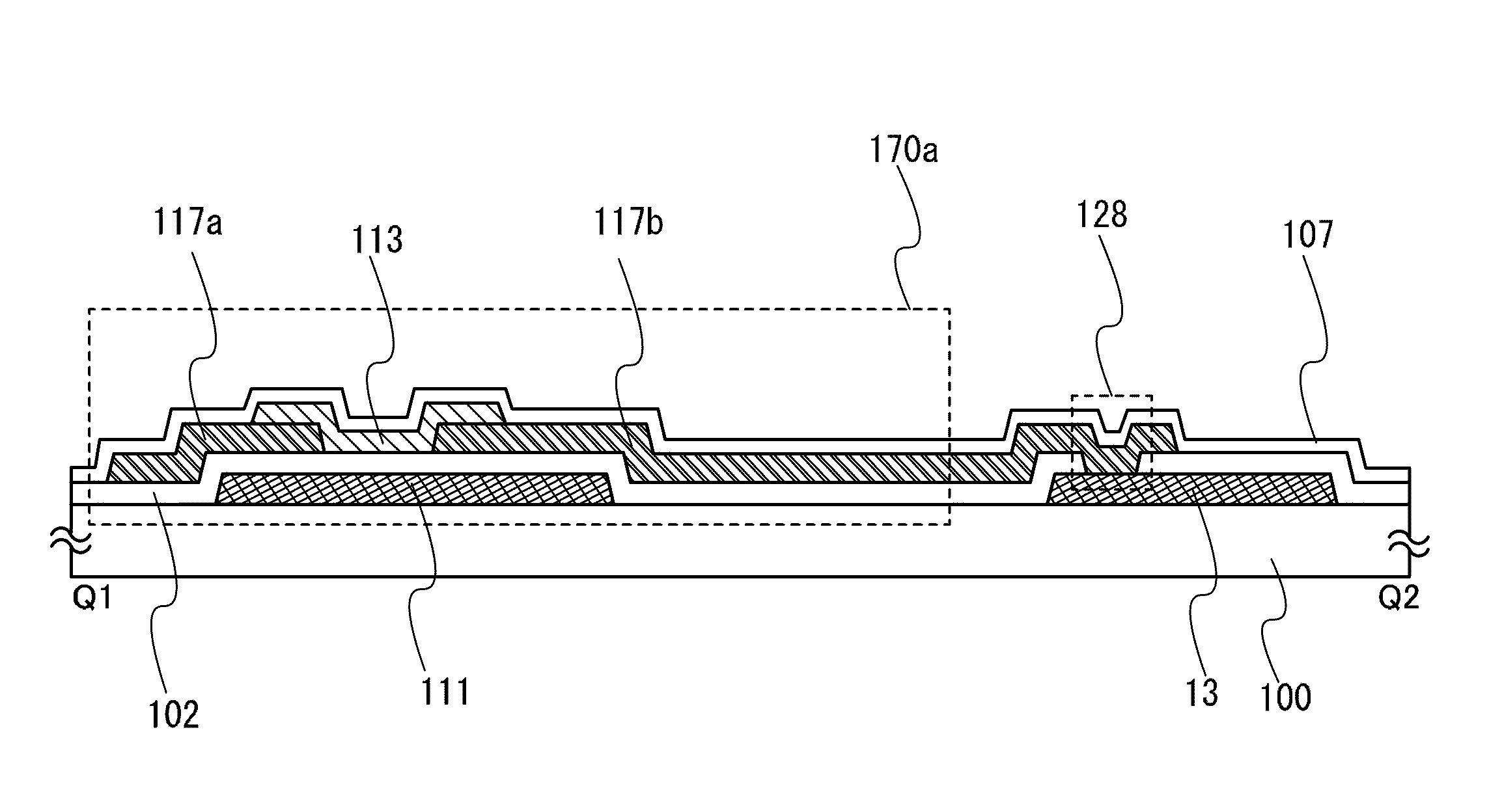
[0071]In this embodiment, an example of a process for manufacturing the protective circuit illustrated in FIG. 4A described in Embodiment 1 is described with reference to FIGS. 6A to 6C and FIGS. 7A to 7C. FIGS. 6A to 6C and FIGS. 7A to 7C are cross-sectional views taken along line Q1-Q2 of FIG. 4A.

[0072]In FIG. 6A, a glass substrate of barium borosilicate glass, aluminoborosilicate glass, aluminosilicate glass, or the like available in the market can be used as a substrate 100 having a light-transmitting property. For example, a glass substrate which includes more barium oxide (BaO) than boric acid (B2O3) in composition ratio and whose strain point is 730° C. or higher is preferable. This is because such a glass substrate is not strained even in the case where the oxide semiconductor layer is thermally processed at high temperatures of about 700° C.

[0073]Next, a conductive film which is to be a gate wiring including the gate electrode 111 and the scan line 13, a capacitor wiring, a...

embodiment 3

[0100]This embodiment illustrates an example of an electronic paper in which a protective circuit and a thin film transistor disposed in a pixel portion are provided over one substrate, as a display device to which an embodiment of the present invention is applied.

[0101]FIG. 10 illustrates an active matrix type electronic paper as an example of a display device to which an embodiment of the present invention is applied. A thin film transistor 581 used for a semiconductor device can be manufactured in a manner similar to the non-linear element described in Embodiment 2, which is a thin film transistor including an oxide semiconductor containing In, Ga, and Zn as a semiconductor layer and having excellent electric characteristics.

[0102]The electronic paper of FIG. 10 is an example of a display device in which a twisting ball display system is employed. The twisting ball display system refers to a method in which spherical particles each colored in black and white are used for a displa...


PUM


Abstract

The protective circuit is formed using a non-linear element which includes a gate insulating film covering a gate electrode; a first wiring layer and a second wiring layer which are over the gate insulating film and whose end portions overlap with the gate electrode; and an oxide semiconductor layer which is over the gate electrode and in contact with the gate insulating film and the end portions of the first wiring layer and the second wiring layer. The gate electrode of the non-linear element and a scan line or a signal line is included in a wiring, the first or second wiring layer of the non-linear element is directly connected to the wiring so as to apply the potential of the gate electrode.

Description

TECHNICAL FIELD[0001]The present invention relates to a display device including an oxide semiconductor.BACKGROUND ART[0002]A thin film transistor formed over a flat plate such as a glass substrate is manufactured using amorphous silicon or polycrystalline silicon, as typically seen in a liquid crystal display device. Thin film transistors manufactured using amorphous silicon have low field effect mobility, but can be formed over a glass substrate with a larger area. On the other hand, thin film transistors manufactured using polycrystalline silicon have high field effect mobility, but a crystallization step such as laser annealing is necessary and are not always suitable for a larger glass substrate.[0003]In view of the foregoing, attention has been drawn to a technique for manufacturing a thin film transistor using an oxide semiconductor, and applying the transistor to an electronic device or an optical device. For example, Patent Document 1 and Patent Document 2 disclose a techni...

Claims


Application Information

Patent Timeline
Patent Type & Authority Patents(United States)
IPC IPC(8): H01L29/04H05B44/00
CPCH01L27/0266H01L27/124H01L29/7869H01L27/1225G02F1/136H01L27/1214
Inventor YAMAZAKI, SHUNPEIAKIMOTO, KENGOKOMORI, SHIGEKIUOCHI, HIDEKIFUTAMURA, TOMOYAKASAHARA, TAKAHIRO
Owner SEMICON ENERGY LAB CO LTD
Why Eureka
Try Eureka