

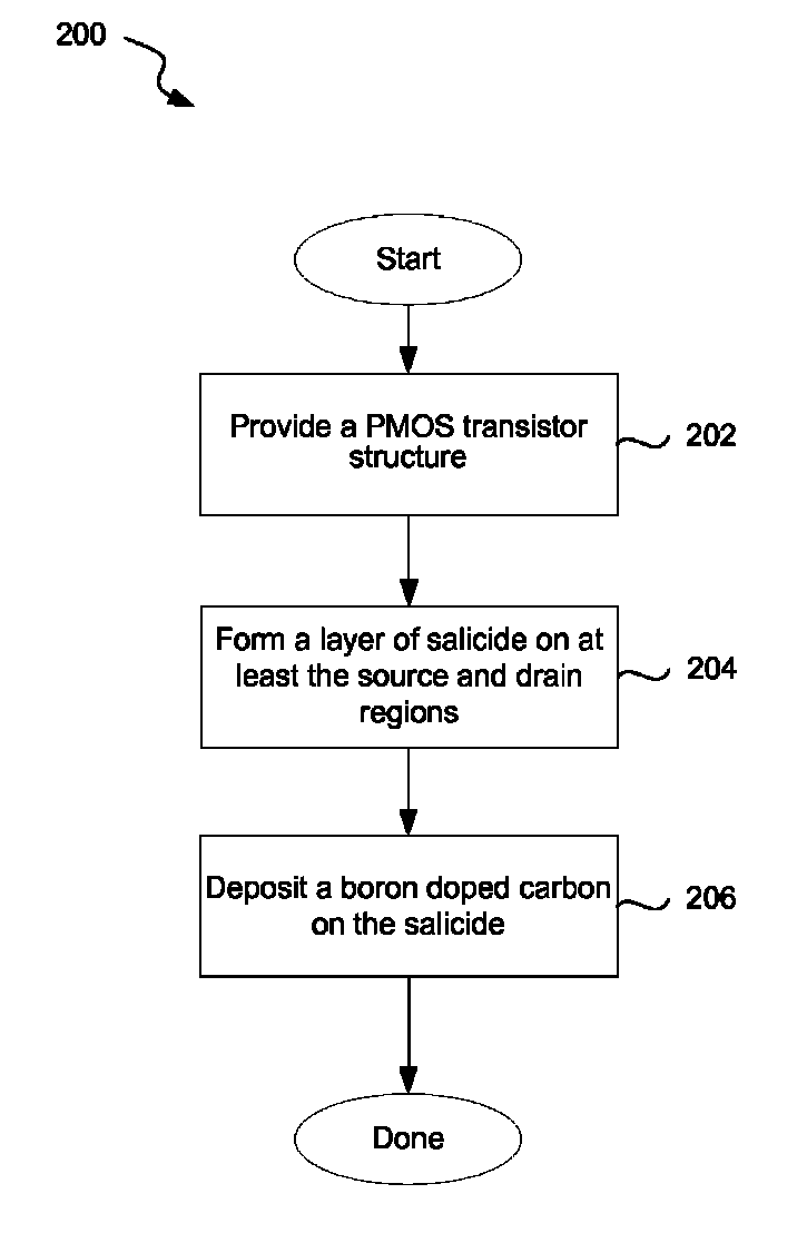
Method for making high stress boron-doped carbon films
a carbon film and high-stress technology, applied in the field of strained transistor architecture of pmos devices, can solve the problems of increasing the resistivity to unacceptable levels, comparing compressive properties, so as to achieve high channel strain without adversely affecting the efficiency of the transistor fabrication process, enhance the performance of the resulting transistor, and preserve the effect of material quality
- Summary
- Abstract
- Description
- Claims
- Application Information
AI Technical Summary
Benefits of technology
Problems solved by technology
Method used
Image

Examples
example
[0059]The following example is provided to further illustrate aspects and advantages of the present invention. This example is provided to exemplify and more clearly illustrate aspects of the present invention and is in no way intended to be limiting.
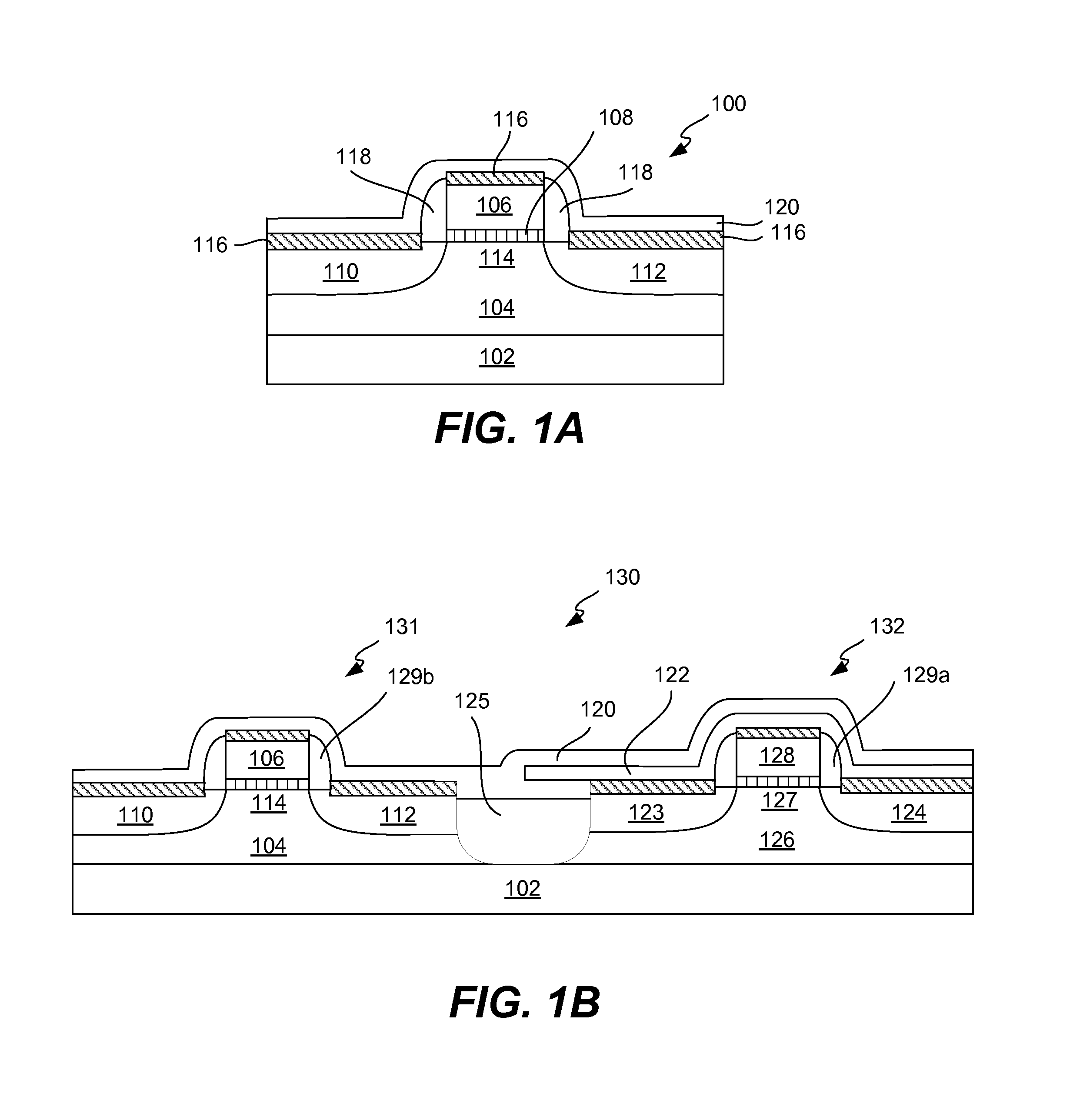
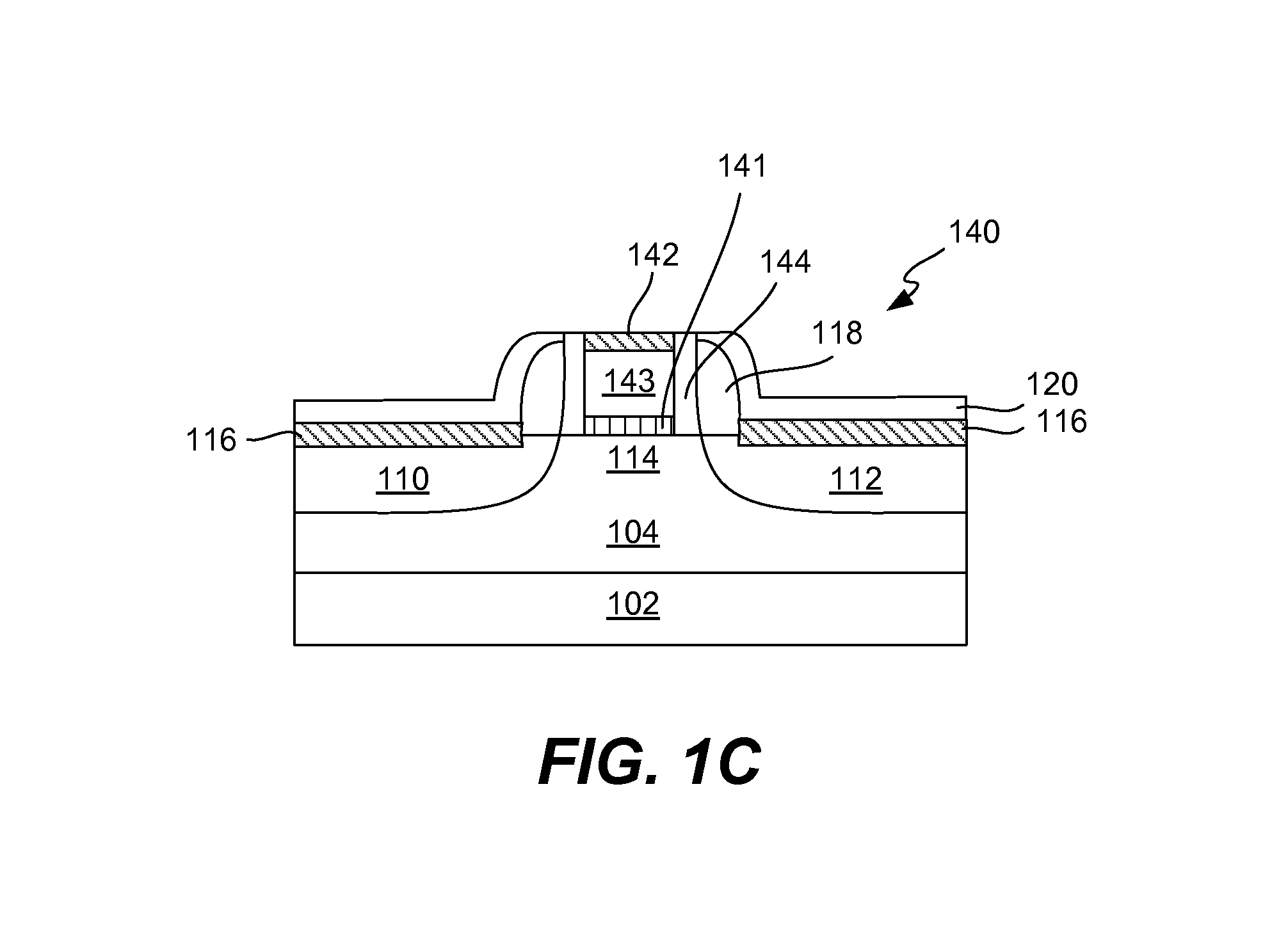
[0060]A boron doped carbon capping layer film was deposited on the silicon substrates of a series of commercially-available silicon semiconductor wafers. The capping layer was deposited on each wafer using a PECVD process in all six RF stations of a Novellus Sequel apparatus. The deposition plasma conditions were the same for all wafers, and are summarized here for the Sequel apparatus as a whole. Flow rates and power values for each of the six RF stations corresponded to about one-sixth of the values listed below.
[0061]The boron containing precursor used was boron tri-fluoride. The flow rate for boron tri-fluoride was 25 sccm. The carbon containing precursor used was methane. The flow rate for methane was 200 sccm. The pressure in the ...
PUM
 Abstract
Description
Claims
Application Information