Electron beam apparatus

a technology of electron beam and apparatus, which is applied in the direction of material analysis, wave/particle radiation treatment, instruments, etc., can solve the problems of increased critical resolution, increased processing speed, and sometimes largely increased processing speed, so as to reduce the influence of space charge effect, increase processing speed, and reduce the light path length of the electron beam apparatus

Active Publication Date: 2011-11-29
KIOXIA CORP
View PDF77 Cites 8 Cited by
  • Summary
  • Abstract
  • Description
  • Claims
  • Application Information

AI Technical Summary

Benefits of technology

[0009]It is another object of the present invention to provide an electron beam apparatus which evaluates a sample at a high throughput and employs a Wien-filter which does not cause a problem of fringe electromagnetic filed.
[0010]It is a further object of the present invention to provide an electron beam apparatus which increases the processing speed by disposing lenses for correcting axial chromatic aberration or spherical aberration in place.
[0011]It is another object of the present invention to provide an electron beam apparatus and a pattern evaluation method which are capable of reducing the influence of space charge effect when a miniaturized pattern is evaluated by reducing the light path length of the electron beam apparatus and reducing the occurrence of deflection aberration.Means for Solving the Problems
[0014]It is also preferable that the secondary electro-optical system is a projection optical system, and the beam separator is adapted to deflect the primary electron beam by a second angle to direct the primary electron beam onto the sample at a third angle which is slightly inclined from a normal of the sample surface, and deflect the second electrons by a first angle which is equal to zero. In this case, it is preferable that the beam separator comprises ferromagnetic material bodies and exciting coils wound around the ferromagnetic material bodies, respectively, and each of the bodies has two magnetic pole surfaces which are magnetically connected to the magnetic surfaces of the other body, and the secondary electro-optical system comprises an axially symmetric shield around an optical axis of the secondary electro-optical system, for preventing a magnetic field generated by the beam separator from introducing into the optical axis.

Problems solved by technology

However, when semiconductor devices are manufactured and / or evaluated using an electron beam apparatus, the processing speed should sometimes be largely increased, inferior to a critical resolution such that the resolution is kept unchanged at several tens of nm.
However, since an axial chromatic aberration correcting lens or a spherical aberration correcting lens used in an electron beam apparatus increases a light path length, a space charge effect is increased, which may cause the processing speed increased.
Conventional electron beam apparatuses, however, are incapable of solving such a problem of space charge effect.
Also, conventional multi-pole aberration correcting lenses can cause additional aberration depending on the field of fringes.
Moreover, no prior art has been found, which uses an NA aperture member having a large opening, and is capable of increasing a beam current, or reducing the space charge effect, by correcting aberration such as axial chromatic aberration and spherical aberration.
This leads to such problems as difficulties in down-sizing the electron beam apparatus due to a longer light path length of the apparatus, blurred images resulting from deflection aberration caused by the beam separator, and the like.
However, such an electron beam apparatus has problems of the inability to generate a large beam current and an extremely small throughput, due to aberration, if the resolution is reduced.
However, when patterns on a sample are miniaturized, if axial chromatic aberration is corrected for operation with a large aperture in order to achieve a high throughput, a problem arises in that a large focus depth cannot be provided.

Method used


Image

  • Electron beam apparatus
  • Electron beam apparatus
  • Electron beam apparatus

Examples


first embodiment

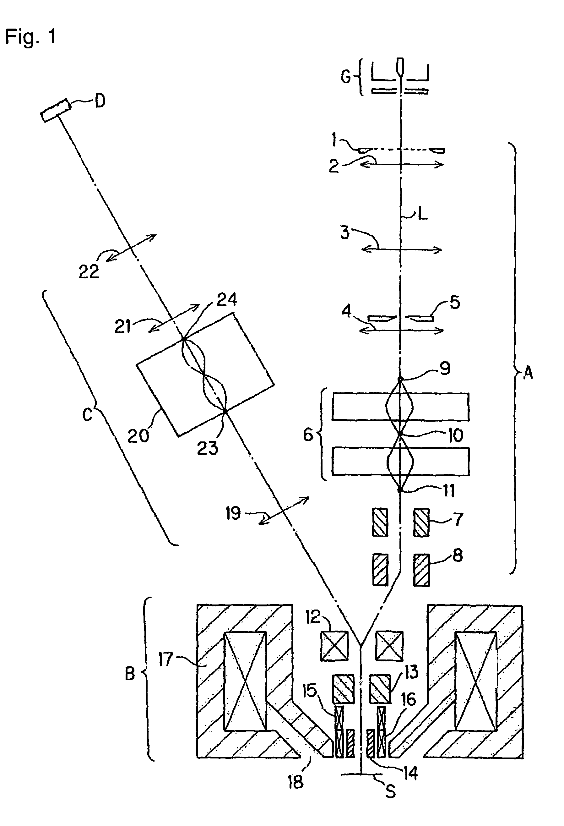
[0044]FIG. 1 is a diagram generally showing an electron beam apparatus according to the present invention. As shown in FIG. 1, the electron beam apparatus comprises: an electron gun G; an electro-optical system A for transporting a primary electron beam emitted from the electron gun G; an electro-optical system B for irradiating a sample S with the primary electron beam sent from the electro-optical system A and separating a secondary electron beam emitted from the sample S from the primary electron beam; an electro-optical system C for transporting the separated secondary electron beam; and a detector D for receiving the secondary electron beam from the electro-optical system C.

[0045]The electro-optical system A comprises a multi-aperture member 1, a condenser lens 2, reduction lenses 3, 4, NA aperture member 5, aberration correcting lens 6, a first scan deflector 7, and a pre-deflector 8 for beam separation. The aberration correction lens 6 comprises, for example, correction lense...

fourth embodiment

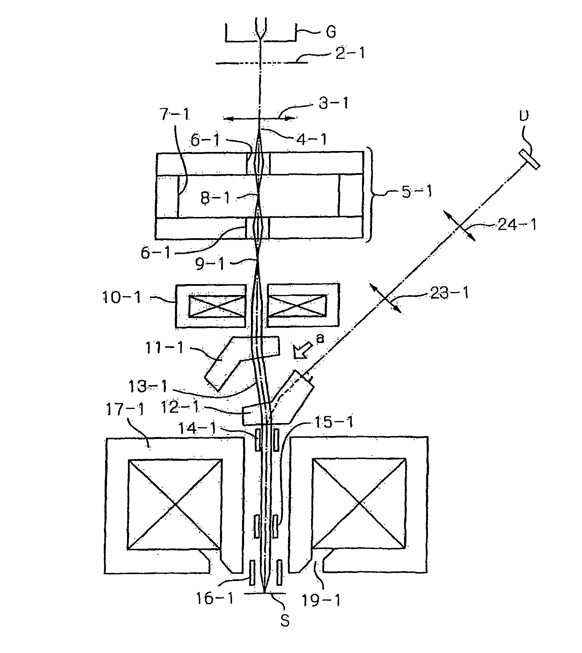
[0083]FIG. 5 shows a schematic diagram of an electron beam apparatus according to the present invention. This embodiment is a multi-beam SEM electron beam apparatus. In this electron beam apparatus, electron beams emitted from an electron gun G is irradiated to a plurality of apertures 2-1, and forms a reduced image at a position 4-1 by a reduction lens 3-1. Then, the electron beams are focused at positions 8-1 and 9-1 by a non-dispersion Wien-filter 5-1 and further reduced in scale by tablet lenses 10-1 and 17-1, and forms a reduced image of multi-beams on a sample S. The tablet lens 17-1 is a magnetic lens which comprises a magnetic gap 19-1 defined on a side of the lens closer to the sample S, and functions as an objective lens.

[0084]Describing in a more specific manner, the Wien-filter 5-1 is configured to perform a convergence action in two regions on the incident side and exiting side in which a bore diameter 6-1 is set smaller, and not to perform a filter action in a central ...

fifth embodiment

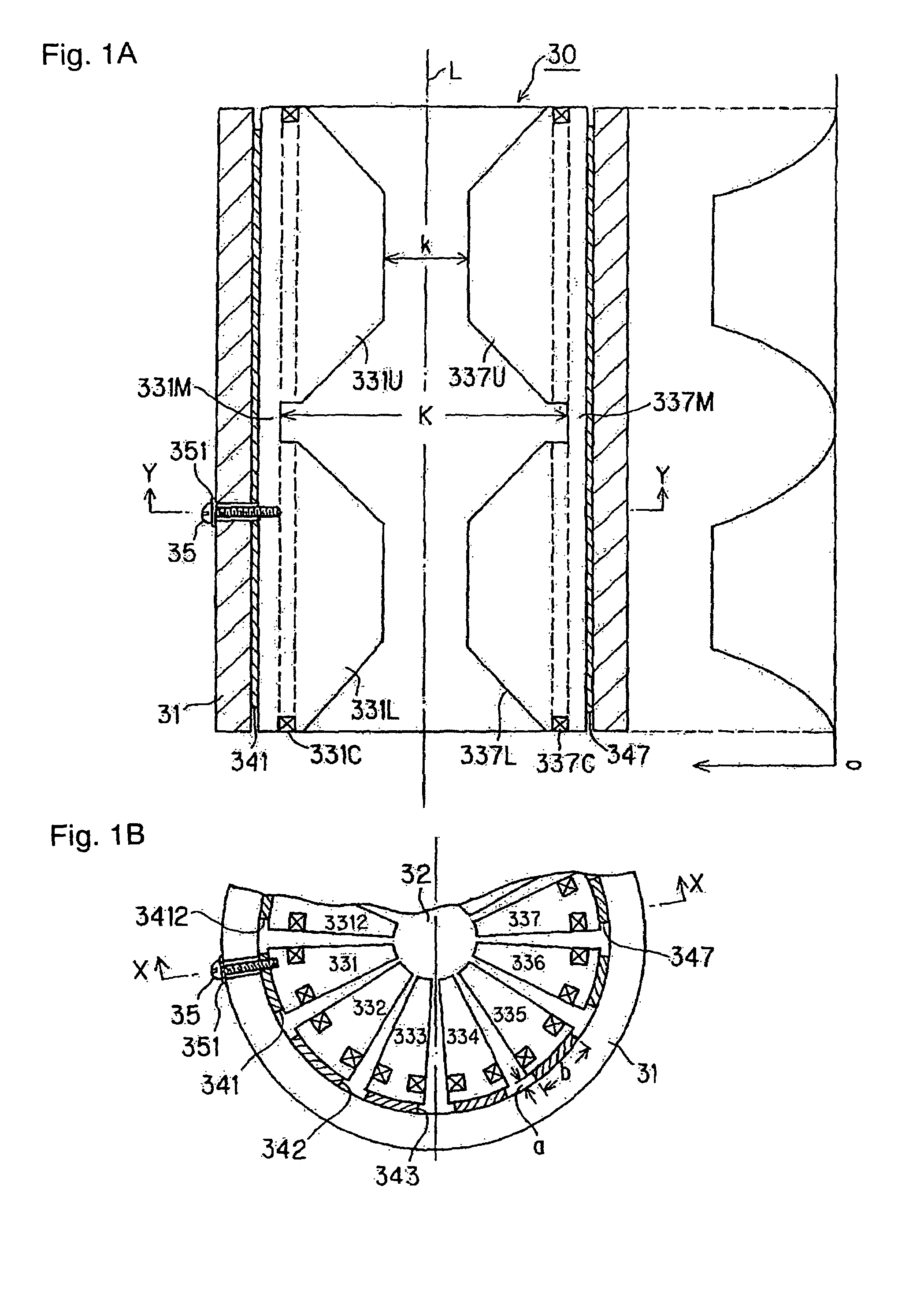
[0094]FIG. 6 shows an electron beam apparatus according to the present invention. In this embodiment, the electron beam apparatus comprises a projection electro-optical system. In this electron beam apparatus, an electron beam emitted from an electron gun G is irradiated to a rectangular aperture 32-1 at a uniform intensity, and a resulting rectangular primary electron beam is adjusted in reduction factor by lenses 33-1 and 34-1 at two stages, and is deflected by an electromagnetic deflector 35-1. Then, it is directed onto a sample S along a trajectory indicated by 38-1 (for example, in a range of 4 to 15°) through an objective lens 36.

[0095]Secondary electrons emitted from the sample S by the irradiation of the primary electron beam pass through the objective lens 36-1, is limited to an appropriate resolution by an NA aperture 40-1, is converged by the tablet lens 42-1, and generates a magnified image at an object point 43-1 of an axial chromatic aberration correcting lens 44-1. Th...


PUM

PropertyMeasurementUnit
widthaaaaaaaaaa
thicknessaaaaaaaaaa
electric fieldaaaaaaaaaa

Abstract

An electron beam emitted from an electron gun (G) forms a reduced image on a sample (S) through a non-dispersion Wien-filter (5-1), an electromagnetic deflector (11-1), a beam separator (12-1), and a tablet lens (17-1) as an objective lens. The beam separator (12-1) is configured such that a distance by which a secondary electron beam passes through the beam separator is approximately three times longer than a distance by which a primary electron beam passes through the beam separator. Therefore, even if a magnetic field in the beam separator is set to deflect the primary electron beam by a small angle equal to or less than approximately 10 degrees, the secondary electron beam can be deflected by approximately 30 degrees, so that the primary and secondary electron beams are sufficiently separated. Also, since the primary electron beam is deflected by a small angle, less aberration occurs in the primary electron beam. Accordingly, since a light path length of a primary electro-optical system, it is possible to reduce the influence of space charge and the occurrence of deflection aberration.

Description

TECHNICAL FIELD[0001]The present invention relates to an electron beam apparatus for evaluating at a high throughput, defect inspections, CD measurements, alignment measurements, and other evaluations for a substrate which has a pattern with a minimum line width of 0.1 μm or less.BACKGROUND ART[0002]As electron beam apparatuses for inspecting patterns on a substrate for defects and the like for evaluation, there are known a scanning electronic microscope (SEM) and a transmission electronic microscope (TEM) which have ultra-high resolutions using axial chromatic aberration correcting lenses. An electron beam apparatus using an axial chromatic aberration correcting lenses is disclosed in Lecture Preliminary Report of 52-th Applied Physics United Meeting (Spring 2005 in Saitama University), p 812 and p 815. Conventional axial chromatic aberration correcting lenses and spherical aberration correcting lenses have four or twelve electrodes or magnetic poles.[0003]Conventionally, such axia...

Claims


Application Information

Patent Timeline
Patent Type & Authority Patents(United States)
IPC IPC(8): G01N23/00
CPCH01J37/05H01J37/147H01J37/153H01J37/26H01J2237/057
Inventor NAKASUJI, MAMORUMURAKAMI, TAKESHISATAKE, TOHRUKARIMATA, TSUTOMIKIMBA, TOSHIFUMIMIYAMOTO, MATSUTAROSOBUKAWA, HIROSHIMORI, SATOSHIYAMAZAKI, YUICHIRONAGAHAMA, ICHIROTA
Owner KIOXIA CORP
Why Eureka
Try Eureka